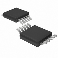
LTC4252A-2IMS#TRPBF Linear Technology, LTC4252A-2IMS#TRPBF Datasheet - Page 12

LTC4252A-2IMS#TRPBF
Manufacturer Part Number
LTC4252A-2IMS#TRPBF
Description
IC CNTRLR HOTSWAP NEGVOLT 10MSOP
Manufacturer
Linear Technology
Type
Hot-Swap Controllerr
Datasheet
1.LTC4252-1CMS8PBF.pdf
(36 pages)
Specifications of LTC4252A-2IMS#TRPBF
Applications
General Purpose
Internal Switch(s)
No
Operating Temperature
-40°C ~ 85°C
Mounting Type
Surface Mount
Package / Case
10-TFSOP, 10-MSOP (0.118", 3.00mm Width)
Lead Free Status / RoHS Status
Lead free / RoHS Compliant
Available stocks
Company
Part Number
Manufacturer
Quantity
Price
OPERATION
LTC4252-1/LTC4252-2
LTC4252A-1/LTC4252A-2
Hot Circuit Insertion
When circuit boards are inserted into a live backplane, the
supply bypass capacitors can draw huge transient currents
from the power bus as they charge. The flow of current
damages the connector pins and glitches the power bus,
causing other boards in the system to reset. The LTC4252
is designed to turn on a circuit board supply in a controlled
manner, allowing insertion or removal without glitches or
connector damage.
Initial Start-Up
The LTC4252 resides on a removable circuit board and
controls the path between the connector and load or power
conversion circuitry with an external MOSFET switch (see
Figure 1). Both inrush control and short-circuit protection
are provided by the MOSFET.
A detailed schematic for the LTC4252A is shown in Figure 2.
– 48V and –48RTN receive power through the longest con-
nector pins and are the first to connect when the board is
inserted. The GATE pin holds the MOSFET off during this
time. UV and OV determine whether or not the MOSFET
should be turned on based upon internal high accuracy
thresholds and an external divider. UV and OV do double
duty by also monitoring whether or not the connector is
seated. The top of the divider detects –48RTN by way of
a short connector pin that is the last to mate during the
insertion sequence.
12
–48RTN
BACKPLANE
–48V
LONG
LONG
Figure 1. Basic LTC4252 Hot Swap Topology
PLUG-IN BOARD
LTC4252
+
C
LOAD
+
–
CONVERTER
ISOLATED
MODULE
DC/DC
–
+
LOW
VOLTAGE
CIRCUITRY
4252-1/2 F01
–48RTN
Interlock Conditions
A start-up sequence commences once these “interlock”
conditions are met.
1. The input voltage V
2. The voltage at UV > V
3. The voltage at OV < V
4. The (SENSE – V
5. The voltage at SS is < 0.2V (20 • V
6. The voltage on the TIMER capacitor (C
7. The voltage at GATE is < 0.5V (V
The first three conditions are continuously monitored and
the latter four are checked prior to initial timing or GATE
ramp-up. Upon exiting an OV condition, the TIMER pin
voltage requirement is inhibited. Details are described in
the Applications Information, Timing Waveforms section.
TIMER begins the start-up sequence by sourcing 5.8μA
into C
cycle stops and TIMER discharges C
waits until the aforementioned conditions are once again
met. If C
and both SS and GATE pins are released. GATE sources
58μA (I
capacitance. The SS voltage ramp limits V
the inrush current. PWRGD pulls active low when GATE is
within 2.8V of V
–48V
SHORT
LONG
LONG
T
. If V
GATE
T
30.1k
**DIODES, INC
†
Figure 2. –48V, 2.5A Hot Swap Controller
392k
successfully charges to 4V, TIMER pulls low
RECOMMENDED FOR HARSH ENVIRONMENTS
1%
1%
), charging the MOSFET gate and associated
R1
R2
IN
, UV or OV falls out of range, the start-up
IN
C1
10nF
DDZ13B**
and DRAIN is lower than V
EE
) voltage is < 50mV (V
IN
D
IN
UVHI
OVLO
exceeds V
+
C
1μF
.
.
IN
C
0.68μF
3 × 1.8k IN SERIES
T
68nF
C
SS
1/4W EACH
LKO
GATEL
OV
UV
TIMER
SS
T
V
EE
OS
to less than 1V, then
0.02Ω
10nF
(UVLO).
T
C
LTC4252A-1
R
R
).
) is < 1V (V
C
S
IN
).
SENSE GATE
SENSE
V
IN
CB
10Ω
R
DRAIN
DRNL
C
IRF530S
).
to control
Q1
C
100μF
LOAD
TMRL
.
425212fc
R
1M
425212 F02
+
D
).


