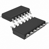
LTC1645CS Linear Technology, LTC1645CS Datasheet - Page 8

LTC1645CS
Manufacturer Part Number
LTC1645CS
Description
IC CTRLR SEQ HOTSWAP DUAL 14SOIC
Manufacturer
Linear Technology
Type
Hot-Swap Controllerr
Datasheet
1.LTC1645CS8PBF.pdf
(24 pages)
Specifications of LTC1645CS
Applications
General Purpose
Internal Switch(s)
No
Voltage - Supply
1.2 V ~ 12 V
Operating Temperature
0°C ~ 70°C
Mounting Type
Surface Mount
Package / Case
14-SOIC (0.154", 3.90mm Width)
Linear Misc Type
Positive Low Voltage
Family Name
LTC1645
Package Type
SOIC N
Operating Supply Voltage (min)
1.2V
Operating Supply Voltage (max)
12V
Operating Temperature (min)
0C
Operating Temperature (max)
70C
Operating Temperature Classification
Commercial
Product Depth (mm)
3.99mm
Product Height (mm)
1.5mm
Mounting
Surface Mount
Pin Count
14
Lead Free Status / RoHS Status
Contains lead / RoHS non-compliant
Lead Free Status / RoHS Status
Contains lead / RoHS non-compliant
Available stocks
Company
Part Number
Manufacturer
Quantity
Price
Part Number:
LTC1645CS
Manufacturer:
LINEAR/凌特
Quantity:
20 000
Part Number:
LTC1645CS#TRPBF
Manufacturer:
LINEAR/凌特
Quantity:
20 000
Part Number:
LTC1645CS8
Manufacturer:
LINEAR/凌特
Quantity:
20 000
Part Number:
LTC1645CS8#TRPBF
Manufacturer:
LT/凌特
Quantity:
20 000
APPLICATIO S I FOR ATIO
LTC1645
Power Supply Ramping
The power supplies on a board are controlled by placing
external N-channel pass transistors in the power paths as
shown in Figure 2. Consult Table 1 for a selection of
N-channel FETs suitable for use with the LTC1645. R
and R
prevent high frequency oscillation. By ramping the gates
of the pass transistors up and down at a controlled rate,
the transient surge current (I = C • dv/dt) drawn from the
main backplane supply is limited to a safe value when the
board makes connection.
When power is first applied to the chip, the gates of the
N-channels (GATE1 and GATE2 pins) are pulled low. After
the ON pin is held above 0.8V for at least one timing cycle,
the voltage at GATE1 begins to rise with a slope equal to
dv/dt = 10 A/C1 (Figure 3), where C1 is the external
capacitor connected between the GATE1 pin and GND. If
the ON pin is brought above 2V (and the ON pin has been
held above 0.8V for at least one timing cycle), the voltage
at GATE2 begins to rise with a slope equal to dv/dt =
10 A/C2.
8
V
V
CC1
CC2
10
4
ON
FAULT
V
SENSE2
R
CC1
SENSE1
14
SENSE1
TIMER
13
11
Figure 2. Typical Hot Swap Connection
provide current fault detection and R1 and R2
C
TIMER
GATE1
Q1
(14-LEAD)
LTC1645
12
R1
10
U
V
C1
CC2
R
SENSE2
1
SENSE2
U
GND
2
7
COMPOUT
GATE2
COMP
RESET
Q2
3
W
R2
10
FB
+
9
8
5
6
C2
U
+
+
SENSE1
C
C
LOAD1
LOAD2
V
V
1645 F02
OUT1
OUT2
The ramp time for each supply is t = (V
the ON pin is pulled below 2V for GATE2 or 0.8V for GATE1
(but above 0.4V), a 40 A current source is connected from
GATE n to GND, and the voltage at the GATE n pin will ramp
down, as shown in Figure 4.
Ringing
Good engineering practice calls for bypassing the supply
rail of any circuit. Bypass capacitors are often placed at the
supply connection of every active device, in addition to one
or more large value bulk bypass capacitors per supply rail.
If power is connected abruptly, the bypass capacitors slow
the rate of rise of voltage and heavily damp any parasitic
resonance of lead or trace inductance working against the
supply bypass capacitors.
The opposite is true for LTC1645 Hot Swap circuits on a
daughterboard. In most cases, on the powered side of the
N-channel FET switches (V
capacitor present. An abrupt connection, produced by
plugging a board into a backplane connector, results in a
fast rising edge applied to the V
V
V
CC n
CC n
+ V
+ V
V
V
GATE
GATE
CC n
CC n
Figure 4. Supply Turning Off
Figure 3. Supply Turning On
SLOPE = 10 A/C
V
OUT n
GATE n
t
1
CC n
t
3
n
) there is no supply bypass
SLOPE = 40 A/C
CC n
line of the LTC1645.
t
4
t
1645 F04
2
CC n
n
1645 F03
• C n )/10 A. If
GATE n
V
OUT n
1645fa


