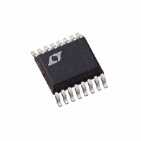
LTC1642CGN Linear Technology, LTC1642CGN Datasheet - Page 14

LTC1642CGN
Manufacturer Part Number
LTC1642CGN
Description
IC CONTROLLER HOTSWAP ADJ 16SSOP
Manufacturer
Linear Technology
Type
Hot-Swap Controllerr
Specifications of LTC1642CGN
Applications
General Purpose, Infiniband™
Internal Switch(s)
No
Voltage - Supply
2.97 V ~ 16.5 V
Operating Temperature
0°C ~ 70°C
Mounting Type
Surface Mount
Package / Case
16-SSOP (0.150", 3.90mm Width)
Linear Misc Type
Positive Low Voltage
Family Name
LTC1642
Package Type
SSOP N
Operating Supply Voltage (min)
2.97V
Operating Supply Voltage (max)
16.5V
Operating Temperature (min)
0C
Operating Temperature (max)
70C
Operating Temperature Classification
Commercial
Product Depth (mm)
3.99mm
Product Height (mm)
1.5mm
Mounting
Surface Mount
Pin Count
16
Lead Free Status / RoHS Status
Contains lead / RoHS non-compliant
Lead Free Status / RoHS Status
Contains lead / RoHS non-compliant
Available stocks
Company
Part Number
Manufacturer
Quantity
Price
Company:
Part Number:
LTC1642CGN
Manufacturer:
LT
Quantity:
10 000
Part Number:
LTC1642CGN
Manufacturer:
LINEAR/凌特
Quantity:
20 000
Part Number:
LTC1642CGN#TRPBF
Manufacturer:
LINEAR/凌特
Quantity:
20 000
LTC1642
APPLICATIO S I FOR ATIO
The undervoltage monitor behaves differently if FB is
above its threshold when the GATE begins ramping:
RESET goes high as soon as the GATE ramp begins.
RESET goes low immediately if V
2.5V internal undervoltage lockout threshold.
To disable the undervoltage monitor, tie FB to REF and
ground RESET.
14
2.5A
12V
V
ALL RESISTORS ±5% UNLESS NOTED.
FB COMPARATOR TRIPS AT V
IN
0.33µF
Figure 12. Undervoltage Monitoring Circuitry
4
C1
ON
RST TMR
V
CC
LTC1642
16
0.015Ω
3
R2
SENSE
GND
RESET
U
GATE
15
8
FB
14
7
5
FDS6630A
OUT
U
Q1
= 10.7V
R3
100Ω
R4
330Ω
C2
0.047µF
CC
Figure 14. Minimum REF Compensation vs REF Current
W
falls below the chip’s
R9
95.3k
1%
R8
12.4k
1%
+
10.0
4.0
2.0
1.0
0.4
0.2
0.1
100µA
D1
1N4705
18V
1642 F12
C
U
LOAD
V
OUT
REFERENCE CURRENT
1mA
Reference
The LTC1642’s internal voltage reference is buffered and
brought out to the REF pin. The buffer amplifier should be
compensated with a capacitor connected between REF
and ground. If no DC current is drawn from REF, 0.1µF
ensures an adequate phase margin, but the minimum
compensation increases if REF sources a substantial DC
current, as shown in Figure 14.
V
20V/DIV
10V/DIV
RSTTMR
1V/DIV
V
RESET
V
IN
1642 F14
Figure 13. Supply Monitor Waveforms
10mA
t
1
t
2
t
3
250ms/DIV
t
4
t
5
1642 F09
1642fb


