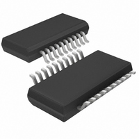
LTC4244IGN-1 Linear Technology, LTC4244IGN-1 Datasheet - Page 20

LTC4244IGN-1
Manufacturer Part Number
LTC4244IGN-1
Description
IC CTRLR HOT SWAP CPCI 20-SSOP
Manufacturer
Linear Technology
Type
Hot-Swap Controllerr
Datasheet
1.LTC4244IGN-1PBF.pdf
(28 pages)
Specifications of LTC4244IGN-1
Applications
CompactPCI™
Internal Switch(s)
No
Voltage - Supply
3.3V, 5V, ±12V
Operating Temperature
-40°C ~ 85°C
Mounting Type
Surface Mount
Package / Case
20-SSOP (0.154", 3.91mm Width)
Family Name
LTC4244-1
Package Type
SSOP N
Operating Supply Voltage (min)
2.25/4.25/10/-10.25V
Operating Supply Voltage (max)
13.5/14.4/-14.4V
Operating Temperature (min)
-40C
Operating Temperature (max)
85C
Operating Temperature Classification
Industrial
Product Depth (mm)
3.99mm
Product Height (mm)
1.5mm
Mounting
Surface Mount
Pin Count
20
Lead Free Status / RoHS Status
Contains lead / RoHS non-compliant
Lead Free Status / RoHS Status
Contains lead / RoHS non-compliant
LTC4244/LTC4244-1
APPLICATIO S I FOR ATIO
Power MOSFET Selection Criteria
The LTC4244 uses external MOSFETs to limit the 5V and
3.3V supply currents. The following criteria should be
used when selecting these MOSFET’s:
1. The on resistance should be low enough to prevent an
2. The drain-to-source breakdown voltage should be high
3. The MOSFET package must be able to handle the
4. The MOSFET package must be able to dissipate the heat
20
excessive voltage drop across the sense resistor and
the series MOSFET at rated load current given the
amount of gate to source voltage provided by the
LTC4244.
enough for the device to survive overvoltage transients
that may occur during fault conditions (the 5V and 3.3V
transient voltage limiters shown in Figure 1 will limit the
maximum drain-source voltage seen by these MOSFET’s
during fault conditions).
maximum, steady state power dissipation for the ON
state without exceeding the device’s rated maximum
junction temperature. The MOSFET’s steady-state, dis-
sipated power can be expressed as:
The increase in steady-state junction-to-ambient tem-
perature is given by:
resulting from the power pulse during the transition
from off to on. A worst-case approximation for the
magnitude of the power pulse is:
where n V
sient current initially charging the load capacitance and
I
of the power pulse can be expressed as:
LOAD
P
T
P
t
J
ON
ON
OFF-ON
– T
is the steady-state load current. The duration, t
= I
A
C
OUT
MAX
= P
LOAD
I
INRUSH
n
2
ON
= 5V
V
• R
OUT
•
U
• R
V
DS(ON)
OUT
OUT
•
JA
or 3.3V
I
U
INRUSH
2
OUT
W
I
LOAD
, I
INRUSH
is the tran-
U
(10)
(11)
ON
(8)
(9)
,
5. The MOSFET package must be able to sustain the
Table 8 lists some power MOSFET’s that can be used with
the LTC4244.
Input Overvoltage Transient Protection
Hot plugging a board into a backplane generates inrush
currents from the backplane power supplies due to the
charging of the plug-in board capacitance. To reduce this
transient current to a safe level, the CPCI Hot Swap
specification restricts the amount of unswitched capaci-
tance used on the input side of the plug-in board. Each
medium or long power pin connected to the CPCI female
connector on the plug-in board is required to have a 10nF
ceramic bypass capacitor to ground. Bulk capacitors are
only allowed on the switched output side of the LTC4244
(5V
tance is allowed on the 5V
planes, but only because a current limiting resistor is
assumed to decouple the connector pin from the bulk
capacitance. Circuits normally placed on the unswitched
side Early Power plane (PCI Bridge, for example) need to
to be decoupled by a current limiting resistor.
Disallowing bulk capacitors on the input power pins miti-
gates the inrush current during Hot Swap. However, it also
tends to create a resonant circuit formed by the inductance
of the backplane power supply trace in series with the
inductance of the connector pin and the parasitic capaci-
tance of the plug-in board (mainly due to the large power
FET). Upon board insertion, the ringing of this circuit can
exhibit a peak overshoot of 2.5 times the steady-state
voltage (>30V for 12V
There are two methods for abating the effects of these high
voltage transients: using voltage limiters to clip the tran-
sient to a safe level and snubber networks. Snubber
networks are series RC networks whose time constants
maximum pulse power that occurs in the event the
LTC4244 attempts to power-up either the 5V or 3.3V
back-end supply into a short circuit (see Design Ex-
ample for a sample calculation).
OUT
, 3.3V
OUT
, 12V
IN
OUT
).
, V
IN
EEOUT
and 3.3V
). Some bulk capaci-
IN
Early Power
42441f


