LTC4244IGN#TR Linear Technology, LTC4244IGN#TR Datasheet - Page 14

LTC4244IGN#TR
Manufacturer Part Number
LTC4244IGN#TR
Description
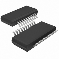
IC CTRLR HOT SWAP CPCI 20-SSOP
Manufacturer
Linear Technology
Type
Hot-Swap Controllerr
Datasheet
1.LTC4244IGN-1PBF.pdf
(28 pages)
Specifications of LTC4244IGN#TR
Applications
CompactPCI™
Internal Switch(s)
No
Voltage - Supply
3.3V, 5V, ±12V
Operating Temperature
-40°C ~ 85°C
Mounting Type
Surface Mount
Package / Case
20-SSOP (0.154", 3.91mm Width)
Lead Free Status / RoHS Status
Contains lead / RoHS non-compliant
Available stocks
Company
Part Number
Manufacturer
Quantity
Price
APPLICATIO S I FOR ATIO
LTC4244/LTC4244-1
Once the power-down sequence is complete, the CPCI
card may be removed from the slot. During extraction, the
precharge circuit continues to bias the bus I/O connector
pins at 1V until the long 5V and 3.3V connector pin
connections are broken.
GATE Pin Capacitor Selection
Both the load capacitance and the LTC4244’s GATE pin
capacitor (C1 in Figure 1) affect the ramp rate of the 5V
and 3.3V
expressed as:
whichever is slowest. The power-up time for any of the
LTC4244’s outputs where the inrush current is constrained
by that supply’s foldback current limit can be approxi-
mated as:
Where n V
example, if C
I
20ms.
If the value of C1 is large enough that it alone determines
the output voltage ramp rate, then the magnitude of the
inrush current initially charging the load capacitance is:
14
LOAD(5VOUT)
I
t
dV
INRUSH
on VOUT
dt
OUT
(
n
OUT
OUT
=
)
I
= 5A, the 5V
I
GATE
C
LIMIT(3.3V)
voltages. The precise relationship can be
C
= 5V
LOAD
LOAD
C
1
I
LIMIT VOUT
1
C
LOAD
OUT
U
or =
=2000 F, I
•
2
(
I
n
GATE
, 3.3V
•
( .
I
3 3
C
–
OUT
LIMIT(5V)
LOAD
U
I
LOAD
VOUT
C
)
turn-on time will be less than
OUT
LOAD VOUT
–
•
I
( .
)
LOAD VOUT
3 3
, 12V
LIMIT(5VOUT)
n
–
(
V
5
V
W
OUT
I
)
LOAD V
(
n
OUT
)
(
5
or V
)
)
= 6A and
U
or
EEOUT
. For
OUT
(1)
(2)
(3)
The maximum power-up time for this condition can be
approximated by:
where V
of the external 5V or 3.3V MOSFET.
In general, the edge rate (dI/dt) at which the back-end 5V
and 3.3V supply currents are turned on can be limited by
increasing the size of C1. Applications that are sensitive to
the edge rate should characterize how varying the size of
C1 reduces dI/dt for the external MOSFET selected for a
particular design.
In the event of a short-circuit or overcurrent condition, the
LTC4244’s GATE pin can be pulled down within 2 s since
a 1k (R5 in Figure 1) decouples C1 from the gates of the
external MOSFET’s (Q1 and Q2 in Figure 1).
TIMER Pin Capacitor Selection
During a power-up sequence, a 21 A current source is
connected to the TIMER pin and current limit faults are
ignored until the voltage ramps to within 1.6V of 12V
This feature allows the part to power up large capacitive
loads using its foldback current limit. The TIMER inhibit
period can be expressed as:
The timer period should be set longer than the duration of
any inrush current that exceeds the LTC4244’s foldback
current limit but yet be short enough not to exceed the
maximum, safe operating area of the external 5V and 3.3V
pass transistors in the event of a short circuit (see Design
Example). As a design aid, the TIMER period as a function
of the timing capacitor using standard values from 0.1 F
to 0.82 F is shown in Table 1.
t
ON
t
TIMER
V
TH,MOSFET(MAX)
OUT
C
TIMER
V
TH MOSFET MAX
,
I
•
GATE MIN
I
12
TIMER
is the maximum threshold voltage
(
V
(
IN
–
)
V
)
TIMER
•
C MAX
1
(
)
42441f
(4)
(5)
IN
.


