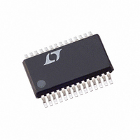
LTC4240IGN#TR Linear Technology, LTC4240IGN#TR Datasheet - Page 21

LTC4240IGN#TR
Manufacturer Part Number
LTC4240IGN#TR
Description
IC CTRLR HOT SWAP CPCI 28-SSOP
Manufacturer
Linear Technology
Type
Hot-Swap Controllerr
Datasheet
1.LTC4240CGNPBF.pdf
(28 pages)
Specifications of LTC4240IGN#TR
Applications
CompactPCI™
Internal Switch(s)
No
Voltage - Supply
3.3V, 5V, ±12V
Operating Temperature
-40°C ~ 85°C
Mounting Type
Surface Mount
Package / Case
28-SSOP (0.150", 3.95mm Width)
Lead Free Status / RoHS Status
Contains lead / RoHS non-compliant
Available stocks
Company
Part Number
Manufacturer
Quantity
Price
APPLICATIO S I FOR ATIO
Transient Power Dissipation
There are certain transient events that can significantly
increase the power dissipated by the external FET. If the
LTC4240 5V supply (at 5V + 10%) powers up into a 1.5V
short (potentially manifested as a short to two diodes in
series), then the FET can potentially have 4V across it with
8.8A flowing. This implies a power dissipation of 35.1W.
The amount of time the FET will dissipate 35.1W will
depend on the relative values of the TIMER and GATE
capacitances. For the values specified on the front page
application circuit, the GATE pin will ramp high signifi-
cantly faster than the TIMER pin, hence transient power
dissipation will be set by the TIMER pin capacitance.
The dissipated 35.1W, the ramp time of the TIMER pin
(50ms will be used for this example), and the FET thermal
resistance will determine the internal junction tempera-
ture of the FET. Most FETs will specify a maximum internal
junction temperature of 150 C. The FET datasheets should
have a transient thermal impedance graph. This graph has
a family of curves listing the FET transient thermal imped-
ance as a function of duty cycle. The duty cycle refers to
what percentage of the time the FET is in the short circuit
condition. If we choose the Si7880DP FET and assume
that the board on which the FET is placed has minimal heat
sinking capability, and further assume that the user will
turn on the board every 2.5 seconds (0.02 duty cycle:
50ms on, 2450ms off), then by looking at the junction-to-
ambient curve we note that with a 70 C ambient tempera-
ture, the Si7880DP internal junction temperature will be
172 C. This is above the absolute maximum rating of the
FET, and although operating at this temperature will not
damage the FET immediately, it does affect its long term
reliability. Conversely, if we assume that there is a perfect
heat sink for the Si7880DP package, then we would use the
junction-to-case curve and calculate a value of 117 C with
a 70 C ambient temperature. The Si7880DP comes in a
thermally enhanced package whose drain lead is a large
piece of metal that can conduct heat away from the internal
junction of the FET. To achieve best performance, the drain
of the Si7880DP should be connected to a piece of copper
(as large as possible) on the board. Note that if the output
is shorted to ground, the current foldback feature will cut
the power dissipation by at least a factor of two.
U
U
W
U
When the LTC4240 is turned on and the large 5V
output capacitor (2000 F or more) is charged, it is pos-
sible that the 5V FET will dissipate as much as the 35.1W
described above. If there is no DC load at 5V
will charge the 2000 F in less than 2ms, which should not
pose any thermal problems for the Si7880DP. If the DC
load at 5V
analysis should be used to calculate the internal junction
temperature of the FET.
Output Voltage Monitor
The DC level of all four supply outputs is monitored by the
power good circuitry. When any of the four supply outputs
falls below its specified level (see DC electrical specifica-
tions) for longer than 10 s, the PWRGD (HEALTHY#)
open drain pin will be deasserted and the LOCAL_PCI_RST#
signal will be asserted low. This does not generate a fault
condition.
The LOCAL_PCI_RST# signal (RESETOUT pin) is derived
from the HEALTHY# (PWRGD pin), PCI_RST# (RESETIN
pin), and Bit 3 of the command latch (see Table 5).
Table 5. LOCAL_PCI_RST# Truth Table
PCI_RST#
LO
X
X
HI
Precharge
The PRECHARGE input and DRIVE output pins are used to
generate the 1V precharge voltage that biases the bus I/O
connector pins during board insertion and extraction
(Figure 10). The LTC4240 is capable of generating
precharge voltages other than 1V. Figure 11 shows a
circuit that can be used in applications requiring a precharge
voltage less than 1V. The circuit in Figure 12 can be used
for applications that need precharge voltages greater than
1V. Table 6 lists suggested resistor values for R11A and
R11B vs precharge voltage for the application circuits
shown in Figures 11 and 12.
OUT
HEALTHY#
approaches the current limit, then the above
LO
HI
X
X
Command Latch
Bit 3 (C3 )
LO
HI
X
X
LTC4240
LOCAL_PCI_RST#
OUT
, then 8.8A
LO
LO
LO
HI
21
OUT
4240f


