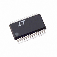
LTC4240IGN#TRPBF Linear Technology, LTC4240IGN#TRPBF Datasheet - Page 17

LTC4240IGN#TRPBF
Manufacturer Part Number
LTC4240IGN#TRPBF
Description
IC CTRLR HOTSWAP CPCI I2C 28SSOP
Manufacturer
Linear Technology
Type
Hot-Swap Controllerr
Datasheet
1.LTC4240CGNPBF.pdf
(28 pages)
Specifications of LTC4240IGN#TRPBF
Applications
CompactPCI™
Internal Switch(s)
No
Voltage - Supply
3.3V, 5V, ±12V
Operating Temperature
-40°C ~ 85°C
Mounting Type
Surface Mount
Package / Case
28-SSOP (0.150", 3.95mm Width)
Lead Free Status / RoHS Status
Lead free / RoHS Compliant
Available stocks
Company
Part Number
Manufacturer
Quantity
Price
APPLICATIO S I FOR ATIO
Note that capacitor C1 performs dual functions. In addi-
tion to controlling the ramp up rates of the 5V and 3.3V
outputs, it also compensates the current limit loop.
Current limit faults are ignored while the TIMER voltage is
less than 5.5V.
Once all four supplies are within tolerance, the PWRGD pin
(HEALTHY#) will be pulled low and LOCAL_PCI_RESET#
(RESETOUT) is free to follow PCI_RST#. Bit 3 of the I
command latch powers up low, thus not asserting
LOCAL_PCI_RST#.
Power-Down Sequence
When either BD_SEL# (OFF/ON) or Bit 2 of the command
latch (C2) is set high, a power-down sequence begins
(Figure 5).
The TIMER pin is immediately pulled low. The GATE pin
(Pin 19) is pulled down by a 200 A current source to
prevent the load currents on the 3.3V and 5V supplies from
going to zero instantaneously and glitching the power
LCL_PCI_RST#
HEALTHY#
BD_SEL#
10V/DIV
10V/DIV
10V/DIV
10V/DIV
10V/DIV
10V/DIV
12V
V
5V/DIV
5V/DIV
5V/DIV
TIMER
5V
3V
EEOUT
GATE
OUT
OUT
OUT
Figure 5. Normal Power-Down Sequence
U
U
10ms/DIV
W
U
4240 F05
2
C
supply voltages. Internal switches are connected to each
of the output supply voltage pins to discharge the output
bulk capacitors to ground. When any one of the output
voltages drops below its PWRGD threshold, the HEALTHY#
signal pulls high, LOCAL_PCI_RST# (RESETOUT) is as-
serted low, and the external status LED turns on.
Once the power-down sequence is complete the status
LED will light up and the CPCI card may be removed from
the slot. During extraction, the precharge circuit will
continue to bias the bus I/O pins at 1V until the long
connector pin connections are broken.
Early Power
Early Power usage is restricted by the CompactPCI (CPCI)
specification. It is intended to power up the precharge
circuit and I/O cells. The CPCI specification allows any of
the long power pins (5V, 3.3V, V(I/O)) to be used for Early
Power. Since Early Power is not isolated, a resistor should
be placed in series with each CPCI connector pin. Note that
if any Early Power pin is shorted on the inserted card, the
current limiting resistor will dissipate the power.
In order to maximize the DC current available from the 5V
supply, all eight 5V connector pins should be tied together
on the inserted card. The same applies to the ten 3.3V CPCI
connector pins. Early Power should then be drawn from
either or both of the two V(I/O) long pins. If either or both
of 5V and 3.3V is used for Early Power, then the 5V and
3.3V sense resistor values must be chosen such that the
1A/pin CPCI rule is not violated.
Connecting V
To lessen the likelihood of faulting on power up, the V
output pin should be bypassed with a capacitor that is only
as large as necessary. A value of 10 F to 47 F is recom-
mended. If a large value bypass capacitor is used (e.g.
power-up or during recovery from power failures.
100 F) on V
EEOUT
EEIN
, current limit faults may occur during
LTC4240
17
EEOUT
4240f


