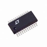
LTC1421CG#PBF Linear Technology, LTC1421CG#PBF Datasheet - Page 8

LTC1421CG#PBF
Manufacturer Part Number
LTC1421CG#PBF
Description
IC CONTROLLER HOT SWAP 24-SSOP
Manufacturer
Linear Technology
Type
Hot-Swap Controllerr
Datasheet
1.LTC1421CG-2.5PBF.pdf
(24 pages)
Specifications of LTC1421CG#PBF
Applications
General Purpose
Internal Switch(s)
No
Voltage - Supply
3 V ~ 12 V
Operating Temperature
0°C ~ 70°C
Mounting Type
Surface Mount
Package / Case
24-SSOP (0.200", 5.30mm Width)
Lead Free Status / RoHS Status
Lead free / RoHS Compliant
Available stocks
Company
Part Number
Manufacturer
Quantity
Price
APPLICATIONS
LTC1421/LTC1421-2.5
Hot Circuit Insertion
When circuit boards are inserted into a live backplane, the
supply bypass capacitors on the board can draw huge
transient currents from the backplane power bus as they
charge up. The transient currents can cause permanent
damage to the connector pins and cause glitches on the
system supply, causing other boards in the system to
reset. At the same time, the system data bus can be
disrupted when the board’s data pins make or break
connection.
The LTC1421 is designed to turn a board’s supply voltages
on and off in a controlled manner, allowing the board to be
safely inserted or removed from a live backplane. The chip
also provides a disable signal for the board’s data bus
buffer during insertion or removal and provides all the
necessary supply supervisory functions for the board.
Power Supply Ramping
The power supplies on a board are controlled by placing
external N-channel pass transistors in the power path
(Figure 3). R1 and R2 provide current fault detection. By
ramping the gate of the pass transistor up at a controlled
rate, the transient surge current (I = C • dV/dt) drawn from
the main backplane supply can be limited to a safe value
when the board makes connection.
12V
When power is first applied to the chip, the gates of both
N-channels, GATELO and GATEHI are pulled low. After the
connection sense pins, CON1 and CON2 are both held low
for at least 20ms, a 20 A reference current is connected
from the RAMP pin to GND. The voltage at GATEHI begins
to rise with a slope equal to 20 A/C
C
8
5V
1
2
RAMP
V
CON1
CON2
3
CCLO
1
23
R1
is an external capacitor connected between the
SETLO GATELO V
2
4
22
Figure 3: Supply Control Circuitry
Q1
21
U
OUTLO
LTC1421
20
V
3
INFORMATION
CCHI
U
1
19
R2
SETHI GATEHI V
2
4
18
RAMP
W
Q2
17
RAMP
(Figure 4), where
OUTHI
16
R
RAMP
10
+
1421 F03
U
+
C
C
LOAD
RAMP
V
V
C
OUTHI
OUTLO
LOAD
RAMP and GATEHI pins. The voltage at the GATEHI pin is
clamped one Schottky diode drop below GATELO.
The ramp time for each supply is equal to: t = (V
(C
pulled down by two internal NFETs.
A negative supply voltage can be controlled using the
CPON pin as shown in Figure 5.
When the board makes connection, the transistor Q3 is
turned off because it’s gate is pulled low to –12V by R4.
CPON is also pulled to –12V. When the charge pump is
turned on, CPON is pulled to V
ramp up with a time constant determined by R4, R5 and
C2. When the charge pump is turned off, CPON goes into
a high impedance state, the gate of Q3 is discharged to V
with a time constant determined by R4 and C2, and Q3
turns off.
CPON
RAMP
V
EE
12V
–12V
–12V
–12V
B
5V
5V
0V
0V
)/20 A. During power down the gates are actively
~1ms
CONNECTOR
–12V FROM
Figure 5. Negative Supply Control
Figure 4. Supplies Turning On
t
1
~1ms
C2
0.047 F
CCLO
R4
20k
5%
1/2 MMDF3N0HD
t
2
and the gate of Q3 will
SLOPE = 20 A/C
LTC1421
CPON
Q3
9
B
R5
16k
5%
+
1421 F4a
RAMP
C
V
V
LOAD
OUTHI
OUTLO
1421 F05
V
–12V
1A
EE
CC
EE
)


