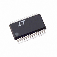
LTC4261CGN Linear Technology, LTC4261CGN Datasheet - Page 26

LTC4261CGN
Manufacturer Part Number
LTC4261CGN
Description
IC CTRLR HOTSWAP W/ADC 28-SSOP
Manufacturer
Linear Technology
Type
Hot-Swap Controllerr
Datasheet
1.LTC4261IGNPBF.pdf
(32 pages)
Specifications of LTC4261CGN
Applications
General Purpose
Internal Switch(s)
No
Voltage - Supply
9 V ~ 11.2 V
Operating Temperature
0°C ~ 70°C
Mounting Type
Surface Mount
Package / Case
28-SSOP (0.150", 3.95mm Width)
Lead Free Status / RoHS Status
Contains lead / RoHS non-compliant
Available stocks
Company
Part Number
Manufacturer
Quantity
Price
Part Number:
LTC4261CGN
Manufacturer:
LINEAR/凌特
Quantity:
20 000
Company:
Part Number:
LTC4261CGN#PBF
Manufacturer:
LT
Quantity:
261
Company:
Part Number:
LTC4261CGN#PBF
Manufacturer:
UNISEM
Quantity:
23 547
Part Number:
LTC4261CGN#PBF
Manufacturer:
LT/凌特
Quantity:
20 000
Part Number:
LTC4261CGN#TRPBF
Manufacturer:
LT/凌特
Quantity:
20 000
Part Number:
LTC4261CGN-2
Manufacturer:
LTNEAR
Quantity:
20 000
Company:
Part Number:
LTC4261CGN-2#PBF
Manufacturer:
LT
Quantity:
102
Company:
Part Number:
LTC4261CGNTRPBF
Manufacturer:
SIEMENS
Quantity:
100
LTC4261/LTC4261-2
APPLICATIONS INFORMATION
(DMY) to measure the internal clock cycle (i.e., the serial
data rate). Following the DMY bit are two channel code bits
CH1 and CH0 labeling the ADC channel (see Table 10). Ten
data bits of the ADC channel (ADC9-0) and three FAULT
register bits (B2, B1 and B0) are then sent out. A parity bit
(PRTY) ends each data stream. After that the SDAO line
enters the idle mode with SDAO pulled high.
The following data reception procedure is recommended:
0. Wait for INTV
1. Wait for SDAO falling edge.
2. The fi rst falling edge could be a glitch, so check again
3. Use the following low-to-high and high-to-low transis-
4. Wait for the second low-to-high transistion (middle of
5. Wait 3/4 of a clock cycle.
6. Sample bit CH1, wait for transistion.
26
after a delay of 10µs. If back to high, wait again. If still
low, it is the START bit.
tions to measure 1/2 of the internal clock cycle.
DMY bit).
CC
rising edge.
7. Wait 3/4 of a clock cycle.
8. Sample bit CH0, wait for transistion.
9. Wait 3/4 of a clock cycle.
10. Sample ADC9, wait for transistion.
11. Continue until all bits are read.
The above procedure can be ported to a microcontroller
or used to design a state machine in FPGA. Code should
have timeouts in case an edge is missed. Abort the read
if it takes more than double the typical time (1.2ms) for
all 18 bits to be clocked out.
A typical application circuit with the LTC4261/LTC4261-2
in the broadcast mode is illustrated in Figure 17, where
input voltage, V
Register Addresses and Contents
The register addresses and contents are summerized in
Table 1 and Table 2. The function of each register bit is
detailed in Tables 3 to 9.
DS
of the FET and V
SENSE
are monitored.
42612fb


