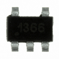
ZXLD1366ET5TA Diodes Zetex, ZXLD1366ET5TA Datasheet - Page 5

ZXLD1366ET5TA
Manufacturer Part Number
ZXLD1366ET5TA
Description
IC LED DRIVR WHITE BCKLGT TSOT-5
Manufacturer
Diodes Zetex
Type
Backlight, White LEDr
Specifications of ZXLD1366ET5TA
Topology
PWM, Step-Down (Buck)
Number Of Outputs
1
Internal Driver
Yes
Type - Primary
Automotive, Backlight
Type - Secondary
High Brightness LED (HBLED), White LED
Frequency
500kHz
Voltage - Supply
6 V ~ 60 V
Voltage - Output
60V
Mounting Type
Surface Mount
Package / Case
TSOT-23-5, TSOT-5, TSOP-5
Operating Temperature
-40°C ~ 125°C
Current - Output / Channel
1A
Internal Switch(s)
Yes
Efficiency
97%
Operating Supply Voltage (typ)
9/12/15/18/24V
Operating Temperature (min)
-40C
Operating Temperature (max)
125C
Operating Temperature Classification
Automotive
Package Type
TSOT-23
Pin Count
5
Mounting
Surface Mount
Power Dissipation
1.8W
Operating Supply Voltage (min)
6V
Lead Free Status / RoHS Status
Lead free / RoHS Compliant
Other names
ZXLD1366E5TA
ZXLD1366E5TR
ZXLD1366E5TR
ZXLD1366E5TR
ZXLD1366E5TR
Available stocks
Company
Part Number
Manufacturer
Quantity
Price
Part Number:
ZXLD1366ET5TA
Manufacturer:
ZETEX
Quantity:
20 000
Device Description
The device, in conjunction with the coil (L1) and current sense resistor (R
converter.
Device operation
(refer to Figure 1 - Block diagram and Figure 2 Operating waveforms)
Operation can be best understood by assuming that the ADJ pin of the device is unconnected and the voltage on this pin
(V
When input voltage V
circuit. Under this condition, the (-) input to the comparator is at ground and its output is high. This turns MN on and switches
the LX pin low, causing current to flow from V
by V
resistor R1 by the current sense circuit and produces a proportional current in internal resistors R2 and R3. This produces a
ground referred rising voltage at the (-) input of the comparator. When this reaches the threshold voltage (V
comparator output switches low and MN turns off. The comparator output also drives another NMOS switch, which bypasses
internal resistor R3 to provide a controlled amount of hysteresis. The hysteresis is set by R3 to be nominally 15% of V
When MN is off, the current in L1 continues to flow via D1 and the LED(s) back to V
determined by the LED(s) and diode forward voltages to produce a falling voltage at the input of the comparator. When this
voltage returns to V
events repeats, with the comparator input ramping between limits of V
Switching thresholds
With V
I
I
Nominal ripple current is ±30mV/R
Adjusting output current
The device contains a low pass filter between the ADJ pin and the threshold comparator and an internal current limiting
resistor (50kΩ nom) between ADJ and the internal reference voltage. This allows the ADJ pin to be overdriven with either
DC or pulse signals to change the V
Details of the different modes of adjusting output current are given in the applications section.
Output shutdown
The output of the low pass filter drives the shutdown circuit. When the input voltage to this circuit falls below the threshold
(0.2V nom.), the internal regulator and the output switch are turned off. The voltage reference remains powered during
shutdown to provide the bias current for the shutdown circuit. Quiescent supply current during shutdown is nominally 60μA
and switch leakage is below 5μA.
ZXLD1366
Document number: DS31992 Rev. 6 - 2
SENSE
OUTnom
ADJ
IN
) appears directly at the (+) input of the comparator.
ADJ
and L1 to produce a voltage ramp (V
pin with respect to V
= 200mV/R
= V
REF
, the ratios of R1, R2 and R3 define an average V
ADJ
S
IN
, the comparator output switches high again. This cycle of
is first applied, the initial current in L1 and R
IN
). The average output current I
S
SENSE
switching threshold and adjust the output current.
SENSE
IN
to ground, via R
) across R
www.diodes.com
OUTnom
5 of 30
S
. The supply referred voltage V
S
, L1 and the LED(s). The current rises at a rate determined
is then defined by this voltage and R
S
SENSE
ADJ
is zero and there is no output from the current sense
± 15%.
S
switching threshold of 200mV (measured on the
), forms a self-oscillating continuous-mode buck
Diodes Incorporated
A Product Line of
IN
. The current decays at a rate
SENSE
is forced across internal
S
according to:
© Diodes Incorporated
ZXLD1366
March 2011
ADJ
ADJ
), the
.


