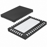
LT3476EUHF#PBF Linear Technology, LT3476EUHF#PBF Datasheet - Page 7

LT3476EUHF#PBF
Manufacturer Part Number
LT3476EUHF#PBF
Description
IC LED DRVR HP CONST CURR 38-QFN
Manufacturer
Linear Technology
Type
High Power, Constant Currentr
Datasheet
1.LT3476EUHFPBF.pdf
(12 pages)
Specifications of LT3476EUHF#PBF
Constant Current
Yes
Topology
PWM, Step-Down (Buck), Step-Up (Boost)
Number Of Outputs
4
Internal Driver
Yes
Type - Primary
Automotive, Backlight
Type - Secondary
Color, RGB
Frequency
200kHz ~ 2MHz
Voltage - Supply
2.8 V ~ 16 V
Voltage - Output
2.2 V ~ 36 V
Mounting Type
Surface Mount
Package / Case
38-QFN
Operating Temperature
-40°C ~ 85°C
Current - Output / Channel
1.5A
Internal Switch(s)
Yes
Efficiency
96%
Led Driver Application
Automotive, Avionic Lighting
No. Of Outputs
4
Output Current
1.5A
Output Voltage
36V
Dimming Control Type
PWM
Rohs Compliant
Yes
Input Voltage
2.8V To 16V
Lead Free Status / RoHS Status
Lead free / RoHS Compliant
Available stocks
Company
Part Number
Manufacturer
Quantity
Price
APPLICATIONS INFORMATION
Layout Hints
The high speed operation of the LT3476 demands careful
attention to board layout. Several items are worthy of note.
The exposed pad of the package is the only GND terminal
of the IC and is also important to thermal management
for the IC, so it is crucial to achieve a good electrical and
thermal contact between the exposed pad and the ground
plane of the board. Also, the Schottky rectifi er and the
capacitor between GND at the cathode of the Schottky
are in the high frequency switching path where current
fl ow is discontinuous. These elements should be placed
so as to minimize the path between SW and the GND of
the IC. To reduce EMI, it is important to minimize the area
of the SW trace. Use a GND plane under SW to minimize
interplane coupling to sensitive signals. To obtain good
current regulation accuracy and eliminate sources of chan-
nel-to-channel coupling, the CAP and LED inputs of each
channel of the LT3476 should be run as separate lines
back to the terminals of the appropriate sense resistor.
Since there is a small DC input bias current (~50μA) to
the LED and CAP inputs, resistance in series with these
inputs should be minimized, otherwise there will be an
offset. Finally, the bypass capacitor on the V
the LT3476 should be placed as close as possible to the
V
Open-Circuit Protection/Overvoltage Lockout
The LT3476 has independent internal overvoltage/open-
circuit protection (OVP) for all four converters, sensed
through their respective CAP inputs. The purpose of the
OVP feature is to protect the main switch of the device
from damage. In the boost confi guration, if the LEDs are
disconnected from the circuit or fail open, the converter
output voltage at CAP is clamped at the OVP voltage of
35V (typ). Figure 1 shows the transient response of the
step-up converter application with LED1 disconnected.
With LED1 disconnected, the converter switches at cur-
rent limit as the output ramps up to OVP . Upon reaching
the OVP clamp voltage, the converter will switch with a
reduced current limit to regulate the converter output
voltage at the OVP clamp. In the buck mode application
shown in the Block Diagram, should the external supply
for CAP exceed the OVP clamp, then switching will be
inhibited for the converter. In order for the overvoltage
IN
terminal of the device.
IN
supply to
protection feature to adequately protect the switch, it is
important that the CAP input sample a voltage at or near
the highest voltage reached by the SW node. As a result,
this OVP function will not provide adequate protection
from open load events in isolated power confi gurations
such as the 1:1 fl yback, since input and output voltage
magnitudes must be summed to obtain the voltage seen
by the switch.
Setting the Switching Frequency
The switching frequency of the LT3476 is set by an ex-
ternal resistor connected between the R
Do not leave this pin open. Also, do not load this pin
with a capacitor. A resistor must always be connected
for proper operation. See Table 1 below or see the Oscil-
lator Frequency vs R
Characteristics for resistor values and corresponding
switching frequencies.
Table 1. Switching Frequency vs R
In general, a lower switching frequency should be used
where either very high or very low switch duty cycle opera-
tion is required, or higher effi ciency is desired. Selection
of a higher switching frequency will allow use of smaller
value external components and yield a smaller solution
size and profi le. Also for high frequency PWM dimming,
a higher switching frequency (shorter switching period)
SWITCHING FREQUENCY (kHz)
V(CAP)
1A/DIV
I(SW)
35V
20V
1000
1200
2000
200
400
0A
Figure 1. LED Disconnect Transient
T
graph in the Typical Performance
LED
DISCONNECT
HERE
20μs/DIV
T
R
T
61.9
16.2
8.25
3476 F01
T
140
21
(kΩ)
pin and GND.
LT3476
3476fa
7


