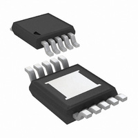
LM3409MY/NOPB National Semiconductor, LM3409MY/NOPB Datasheet - Page 12

LM3409MY/NOPB
Manufacturer Part Number
LM3409MY/NOPB
Description
IC LED DRIVR HIGH BRIGHT 10-MSOP
Manufacturer
National Semiconductor
Series
PowerWise®r
Type
HBLED Driverr
Datasheet
1.LM3409MYNOPB.pdf
(30 pages)
Specifications of LM3409MY/NOPB
Constant Current
Yes
Topology
PWM, Step-Down (Buck)
Number Of Outputs
1
Internal Driver
No
Type - Primary
Automotive
Type - Secondary
High Brightness LED (HBLED)
Voltage - Supply
6 V ~ 42 V
Mounting Type
Surface Mount
Package / Case
10-MSOP Exposed Pad, 10-HMSOP, 10-eMSOP
Operating Temperature
-40°C ~ 125°C
Internal Switch(s)
Yes
Efficiency
97%
Lead Free Status / RoHS Status
Lead free / RoHS Compliant
Voltage - Output
-
Frequency
-
Current - Output / Channel
-
Other names
LM3409MYTR
Available stocks
Company
Part Number
Manufacturer
Quantity
Price
Part Number:
LM3409MY/NOPB
Manufacturer:
TI/德州仪器
Quantity:
20 000
www.national.com
PWM DIMMING USING THE EN PIN
The enable pin (EN) is a TTL compatible input for PWM dim-
ming of the LED. A logic low (below 0.5V) at EN will disable
the internal driver and shut off the current flow to the LED
array. While the EN pin is in a logic low state the support cir-
cuitry (driver, bandgap, V
to minimize the time needed to turn the LED array back on
when the EN pin sees a logic high (above 1.74V).
Figure 7
where duty cycle (D
riod (T
T
LED current (I
The LED current rise and fall times (which are limited by the
slew rate of the inductor as well as the delay from activation
of the EN pin to the response of the external PFET) limit the
achievable T
should be at least one order of magnitude lower than the
steady state switching frequency in order to prevent aliasing.
However, for good linear response across the entire dimming
range, the dimming frequency may need to be even lower.
HIGH VOLTAGE NEGATIVE BIAS REGULATOR
The LM3409/09HV contains an internal linear regulator where
the steady state VCC pin voltage is typically 6.2V below the
voltage at the VIN pin. The VCC pin should be bypassed to
the VIN pin with at least 1µF of ceramic capacitance connect-
ed as close as possible to the IC.
INPUT UNDER-VOLTAGE LOCKOUT (UVLO)
Under-voltage lockout is set with a resistor divider from V
GND and is compared against a 1.24V threshold as shown in
Figure
rising threshold (and assuming the part is enabled), the inter-
nal circuitry becomes active and a 22µA current source at the
UVLO pin is turned on. This extra current provides hysteresis
to create a lower UVLO falling threshold. The resistor divider
is chosen to set both the UVLO rising and falling thresholds.
DIM
, the PFET is disabled. The resulting dimmed average
DIM
8. Once the input voltage is above the preset UVLO
shows the LED current (i
) that the PFET is switching. For the remainder of
DIM
DIM-LED
and D
DIM
) is:
) is the percentage of the dimming pe-
DIM
CC
. In general, dimming frequency
regulator) remains active in order
FIGURE 7. LED Current i
LED
(t)) during PWM dimming
IN
LED
to
(t) During EN Pin PWM Dimming
12
The turn-on threshold (V
The hysteresis (V
LOW POWER SHUTDOWN
The LM3409/09HV can be placed into a low power shutdown
(typically 110µA) by grounding the EN terminal (any voltage
below 0.5V) until V
(typically 3.73V). During normal operation this terminal should
be tied to a voltage above 1.74V and below absolute maxi-
mum input voltage rating.
THERMAL SHUTDOWN
Internal thermal shutdown circuitry is provided to protect the
IC in the event that the maximum junction temperature is ex-
ceeded. The threshold for thermal shutdown is 160°C with 15°
C of hysteresis (both values typical). During thermal shut-
down the PFET and driver are disabled.
FIGURE 8. UVLO Circuit
HYS
CC
) is defined as follows:
drops below the V
TURN-ON
) is defined as follows:
30085614
CC
UVLO threshold
30085613


