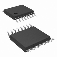
LM3421MH/NOPB National Semiconductor, LM3421MH/NOPB Datasheet - Page 12

LM3421MH/NOPB
Manufacturer Part Number
LM3421MH/NOPB
Description
IC LED DRVR HP CONS CURR 16TSSOP
Manufacturer
National Semiconductor
Series
PowerWise®r
Type
High Power, Constant Currentr
Datasheet
1.LM3421MHNOPB.pdf
(48 pages)
Specifications of LM3421MH/NOPB
Constant Current
Yes
Topology
PWM, SEPIC, Step-Down (Buck), Step-Up (Boost)
Number Of Outputs
1
Internal Driver
No
Type - Primary
Automotive
Type - Secondary
High Brightness LED (HBLED)
Frequency
2MHz
Voltage - Supply
4.5 V ~ 75 V
Voltage - Output
3 V ~ 72 V
Mounting Type
Surface Mount
Package / Case
16-TSSOP Exposed Pad, 16-eTSSOP, 16-HTSSOP
Operating Temperature
-40°C ~ 125°C
Current - Output / Channel
1A
Internal Switch(s)
No
Efficiency
95%
Lead Free Status / RoHS Status
Lead free / RoHS Compliant
Other names
*LM3421MH/NOPB
LM3421MH
LM3421MH
www.national.com
AVERAGE LED CURRENT
The LM3421/23 uses an external current sense resistor
(R
current (I
HSP and HSN pins are the inputs to the high-side sense am-
plifier which are forced to be equal potential (V
through negative feedback. Because of this, the V
is forced across R
which flows out of the CSH pin and through the R
The error amplifier will regulate the CSH pin to 1.24V, there-
fore I
This means V
I
The selection of the three resistors (R
not arbitrary. For matching and noise performance, the sug-
gested signal current I
current does not flow in the LEDs and will not affect either the
off-state LED current or the regulated LED current. I
be above or below this value, but the high-side amplifier offset
characteristics may be affected slightly. In addition, to mini-
mize the effect of the high-side amplifier voltage offset on LED
current accuracy, the minimum V
50 mV. Finally, a resistor (R
series with the HSN pin to cancel out the effects of the input
bias current (~10 µA) of both inputs of the high-side sense
amplifier.
The sense resistor (R
ries string of LEDs as long as the voltage at the HSN and HSP
pins (V
Typically, for a buck-boost configuration, R
bottom of the string (LED-) which allows for greater flexibility
of input and output voltage. However, if there is substantial
input voltage ripple allowed, it can help to place R
top of the string (LED+) which limits the output voltage of the
string to:
Note that he CSH pin can also be used as a low-side current
sense input regulated to 1.24V. The high-side sense amplifier
is disabled if HSP and HSN are tied to AGND (or V
V
LED
HSP
SNS
can then be calculated:
) .
CSH
) placed in series with the LED load to convert the LED
HSP
LED
can be calculated:
and V
) into a voltage (V
SNS
HSN
will be regulated as follows:
HSP
) satisfies the following conditions.
SNS
to generate the signal current (I
CSH
) can be placed anywhere in the se-
HSN
is approximately 100 µA. This
SNS
= R
) as shown in
SNS
HSP
SNS
) should be placed in
is suggested to be
, R
SNS
CSH
is placed at the
Figure
, and R
CSH
SNS
HSP
SNS
resistor.
CSH
voltage
=V
4. The
HSP
at the
HSN
HSN
CSH
can
) is
>
)
)
12
ANALOG DIMMING
The CSH pin can be used to analog dim the LED current by
adjusting the current sense voltage (V
different methods to adjust V
1.
2.
In general, analog dimming applications require a lower
switching frequency to minimize the effect of the leading edge
blanking circuit. As the LED current is reduced, the output
voltage and the duty cycle decreases. Eventually, the mini-
mum on-time is reached. The lower the switching frequency,
the wider the linear dimming range.
CSH methods are physically implemented.
Method 1 uses an external potentiometer in the CSH path
which is a simple addition to the existing circuitry. However,
the LEDs cannot dim completely because there is always
some resistance causing signal current to flow. This method
is also susceptible to noise coupling at the CSH pin since the
potentiometer increases the size of the signal current loop.
Method 2 provides a complete dimming range and better
noise performance, though it is more complex. It consists of
a PNP current mirror and a bias network consisting of an NPN,
2 resistors and a potentiometer (R
the amount of current sourced into the CSH pin. A higher re-
sistance value will source more current into the CSH pin
causing less regulated signal current through R
ly dimming the LEDs. V
voltage reference, while Q7 and Q8 should be a dual pair PNP
for best matching and performance. The additional current
(I
The corresponding I
ADD
External variable resistance : Adjust a potentiometer
placed in series with R
External variable current source: Source current (0 µA to
I
) sourced into the CSH pin can be calculated:
CSH
) into the CSH pin to adjust V
FIGURE 5. Analog Dimming Circuitry
LED
for a specific I
REF
CSH
SNS
should be a precise external
to vary V
using the CSH pin:
ADJ
Figure 5
SNS
SNS
), where R
ADD
SNS
). There are several
.
is:
.
shows how both
HSP
ADJ
, effective-
controls
300673k3


