CAT4109V-GT2 ON Semiconductor, CAT4109V-GT2 Datasheet - Page 7
CAT4109V-GT2
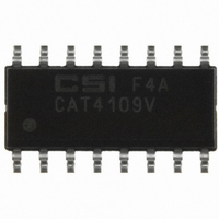
Manufacturer Part Number
CAT4109V-GT2
Description
IC LED DRIVER RGB 16-SOIC
Manufacturer
ON Semiconductor
Type
RGB LED Driverr
Datasheet
1.CAT4109V-GT2.pdf
(12 pages)
Specifications of CAT4109V-GT2
Constant Current
Yes
Topology
PWM
Number Of Outputs
3
Internal Driver
Yes
Type - Primary
Backlight
Type - Secondary
RGB
Voltage - Supply
3 V ~ 5.5 V
Voltage - Output
25V
Mounting Type
Surface Mount
Package / Case
16-SOIC (3.9mm Width)
Operating Temperature
-40°C ~ 85°C
Current - Output / Channel
175mA
Internal Switch(s)
No
Operating Supply Voltage (typ)
3.3/5V
Operating Temperature (min)
-40C
Operating Temperature (max)
85C
Operating Temperature Classification
Industrial
Package Type
SOIC
Pin Count
16
Mounting
Surface Mount
Operating Supply Voltage (min)
3V
Operating Supply Voltage (max)
5.5V
Number Of Digits
3
Low Level Output Current
175 mA
High Level Output Current
200 mA
Operating Supply Voltage
3 V to 5.5 V
Maximum Supply Current
10 mA
Maximum Operating Temperature
+ 85 C
Mounting Style
SMD/SMT
Minimum Operating Temperature
- 40 C
Lead Free Status / RoHS Status
Lead free / RoHS Compliant
Frequency
-
Efficiency
-
Lead Free Status / Rohs Status
Compliant
Other names
CAT4109V-GT2TR


Pin Function
PGND is the power ground reference pin for the device.
This pin must be connected to the GND pin and to the ground
plane on the PCB.
GND is the ground reference pin for the entire device. This
pin must be connected to the ground plane on the PCB.
PWM1 to PWM3 are the control inputs respectively for
LED1, LED2 and LED3 channels. When PWMx are low, the
associated LED channels are turned off. When PWMx are
high, the corresponding channels are turned on, assuming
the OE input is also high. PWMx pins can not be left open
and must be set either to logic high or low.
RSET1 to RSET3 are the LED current set inputs. The
current pulled out of these pins will be mirrored in the
corresponding LED channel with a gain of 400.
LED1 to LED3 are the LED current sink inputs. These pins
are connected to the bottom cathodes of the LED strings.
Table 5. PIN DESCRIPTIONS
RSET3
RSET2
RSET1
PWM3
PWM2
PWM1
PGND
Name
LED3
LED2
LED1
GND
VDD
NC
NC
NC
OE
Pin Number
10
12
13
14
15
16
11
1
2
3
4
5
6
7
8
9
Power Ground.
Ground Reference.
PWM control input for LED3
PWM control input for LED2
PWM control input for LED1
LED current set pin for LED3
LED current set pin for LED2
LED current set pin for LED1
LED channel 3 cathode terminal
LED channel 2 cathode terminal
LED channel 1 cathode terminal
Not connected inside package
Not connected inside package
Not connected inside package
Output Enable input pin
Device Supply pin
http://onsemi.com
7
The current sinks bias the LEDs with a current equal to 400
times the corresponding RSETx pin current. For the LED
sink to operate correctly the voltage on the LED pin must be
above 0.4 V. Each LED channel can withstand voltages up
to 25 V.
OE is the output enable input. When high, all LED channels
are enabled according to the state of their corresponding
PWMx control inputs. When low, all LED channels are
turned off. This pin can be used to turn all the LEDs off
independently of the state of the PWMx inputs. If the OE
stays low for a duration longer than t
enters shutdown mode.
VDD is the positive supply pin voltage for the entire device.
A small 1 mF bypass ceramic capacitor is recommended
between VDD pin and ground near the device.
Function
PWRDWN
, the device
Related parts for CAT4109V-GT2
Image
Part Number
Description
Manufacturer
Datasheet
Request
R

Part Number:
Description:
3-channel Constant-current Rgb Led Driver With Individual Pwm Dimming
Manufacturer:
ON Semiconductor
Datasheet:
Part Number:
Description:
ON Semiconductor [VOLTAGE REGULATOR]
Manufacturer:
ON Semiconductor
Datasheet:
Part Number:
Description:
357-036-542-201 CARDEDGE 36POS DL .156 BLK LOPRO
Manufacturer:
ON Semiconductor
Datasheet:
Part Number:
Description:
357-036-542-201 CARDEDGE 36POS DL .156 BLK LOPRO
Manufacturer:
ON Semiconductor
Datasheet:
Part Number:
Description:
357-036-542-201 CARDEDGE 36POS DL .156 BLK LOPRO
Manufacturer:
ON Semiconductor
Datasheet:
Part Number:
Description:
357-036-542-201 CARDEDGE 36POS DL .156 BLK LOPRO
Manufacturer:
ON Semiconductor
Datasheet:
Part Number:
Description:
357-036-542-201 CARDEDGE 36POS DL .156 BLK LOPRO
Manufacturer:
ON Semiconductor
Datasheet:
Part Number:
Description:
357-036-542-201 CARDEDGE 36POS DL .156 BLK LOPRO
Manufacturer:
ON Semiconductor
Datasheet:
Part Number:
Description:
357-036-542-201 CARDEDGE 36POS DL .156 BLK LOPRO
Manufacturer:
ON Semiconductor
Datasheet:
Part Number:
Description:
357-036-542-201 CARDEDGE 36POS DL .156 BLK LOPRO
Manufacturer:
ON Semiconductor
Datasheet:
Part Number:
Description:
357-036-542-201 CARDEDGE 36POS DL .156 BLK LOPRO
Manufacturer:
ON Semiconductor
Datasheet:
Part Number:
Description:
357-036-542-201 CARDEDGE 36POS DL .156 BLK LOPRO
Manufacturer:
ON Semiconductor
Datasheet:
Part Number:
Description:
Manufacturer:
ON Semiconductor
Datasheet:
Part Number:
Description:
Manufacturer:
ON Semiconductor
Datasheet: