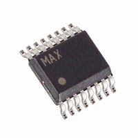
MAX6966AEE+ Maxim Integrated Products, MAX6966AEE+ Datasheet - Page 26

MAX6966AEE+
Manufacturer Part Number
MAX6966AEE+
Description
IC LED DRIVER LINEAR 16-QSOP
Manufacturer
Maxim Integrated Products
Type
Linear (Serial Interface)r
Datasheet
1.MAX6966ATE.pdf
(29 pages)
Specifications of MAX6966AEE+
Constant Current
Yes
Topology
Open Drain, PWM
Number Of Outputs
10
Internal Driver
Yes
Type - Primary
Backlight
Type - Secondary
RGB, White LED
Frequency
270kHz ~ 450kHz
Voltage - Supply
2.25 V ~ 3.6 V
Voltage - Output
7V
Mounting Type
Surface Mount
Package / Case
16-QSOP
Operating Temperature
-40°C ~ 125°C
Current - Output / Channel
20mA
Internal Switch(s)
Yes
Number Of Segments
10
Low Level Output Current
21.1 mA
Operating Supply Voltage
2.25 V to 3.6 V
Maximum Supply Current
730 uA
Maximum Power Dissipation
667 mW
Maximum Operating Temperature
+ 125 C
Mounting Style
SMD/SMT
Minimum Operating Temperature
- 40 C
Lead Free Status / RoHS Status
Lead free / RoHS Compliant
Efficiency
-
Lead Free Status / Rohs Status
Details
In run mode, the output port goes low, approaching 0V,
as the port’s static constant current saturates trying to
sink a higher current than the 220kΩ pullup resistor
can source.
In shutdown mode, the output goes high impedance
together with any other constant-current outputs. This
output remains low during ramp-up and fade-down
sequences because the current drawn by the 220kΩ
pullup resistor is much smaller than the available output
constant current, even at the lowest fade current step.
The MAX6966/MAX6967 can be used to drive loads
needing more than 20mA, like high-current white LEDs,
by paralleling outputs. For example, consider a white
LED that needs to be driven with 70mA. This LED can
10-Port Constant-Current LED Drivers and I/O
Expanders with PWM Intensity Control
26
Driving Load Currents Higher than 20mA
______________________________________________________________________________________
TOP VIEW
µC
SCLK
MOSI
MISO
CS
SCLK
DIN
CS
V+
SCLK
DIN
DOUT
CS
13
14
15
16
MAX6966
12
1
+3.3V
GND
THIN QFN
MAX6966ATE
MAX6967ATE
V+
11
2
10
3
P0
P1
P2
P3
P4
P5
P6
P7
P8
P9
9
4
8
7
6
5
LOGIC INPUT
P6
P5
GND
P4
+5V
D1
be driven using ports P0, P1, P2, and P3 connected in
parallel (shorted together). Three of the ports should be
configured for full current (20mA), and the last port
should be configured for half current (10mA) to meet
the 70mA requirement. The four ports can be controlled
simultaneously with one write access using register
0x0B
have current limiting, they do not have to be switched
simultaneously to ensure safe current sharing.
The MAX6966/MAX6967 operate with a power-supply
voltage of 2.25V to 3.6V. Bypass the power supply to
GND with a 0.1µF ceramic capacitor as close to the
device as possible. For the TQFN version, connect the
underside exposed pad to GND.
(Table
SCLK
GND
CS
P0
P1
P2
P3
P4
1
2
3
4
5
6
7
8
Typical Application Circuit
+5V
6). Note that because the output ports
MAX6966ATE
MAX6967ATE
D2
QSOP
Power-Supply Considerations
Pin Configurations
16
15
14
13
12
11
10
9
V+
DIN
DOUT/OSC
P9
P8
P7
P6
P5
+5V
D3


