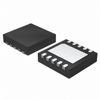
LTC3454EDD#PBF Linear Technology, LTC3454EDD#PBF Datasheet - Page 5

LTC3454EDD#PBF
Manufacturer Part Number
LTC3454EDD#PBF
Description
IC LED DRIVER PHOTO FLASH 10-DFN
Manufacturer
Linear Technology
Type
Photo Flash LEDr
Datasheet
1.LTC3454EDDPBF.pdf
(12 pages)
Specifications of LTC3454EDD#PBF
Topology
PWM, Step-Down (Buck), Step-Up (Boost)
Number Of Outputs
1
Internal Driver
Yes
Type - Primary
Backlight, Flash/Torch
Type - Secondary
White LED
Frequency
900MHz ~ 1.15MHz
Voltage - Supply
2.7 V ~ 5.5 V
Voltage - Output
5.15V
Mounting Type
Surface Mount
Package / Case
10-DFN
Operating Temperature
-40°C ~ 85°C
Current - Output / Channel
1A
Internal Switch(s)
Yes
Efficiency
90%
Led Driver Application
Flashlight, Digital Cameras, PDAs
No. Of Outputs
1
Output Current
1A
Output Voltage
5.35V
Input Voltage
2.7V To 5.5V
Rohs Compliant
Yes
Lead Free Status / RoHS Status
Lead free / RoHS Compliant
Available stocks
Company
Part Number
Manufacturer
Quantity
Price
EN1 (Pin 1): Enable Input Pin for I
EN2 (Pin 2): Enable Input Pin for I
I
to ground programs the current through the LED to I
= 3850(0.8V/R
amount set by EN2/I
I
to ground programs the current through the LED to I
= 3850(0.8V/R
amount set by EN1/I
LED (Pin 5): Low Dropout Output for LED Current Biasing.
Connect the LED between V
SW2 (Pin 6): Switching Node. External inductor con-
nects between SW1 and SW2. Recommended value is
4.7μH/5μH.
TYPICAL PERFORMANCE CHARACTERISTICS
PIN FUNCTIONS
SET1
SET2
(Pin 3): LED Current Programming Pin. A resistor
(Pin 4): LED Current Programming Pin. A resistor
20mV/DIV
ISET1
ISET2
1100
1080
1060
1040
1020
1000
980
960
940
920
900
–55
Output Voltage Ripple
Back Page Application
). This amount of current adds to any
). This amount of current adds to any
Oscillator Frequency vs Temperature
V
I
LED
V
SET2
SET1
IN
OUT
–35
= 3.6V
= 500mA
= 3V
–15
if used.
if used.
OUT
V
V
TEMPERATURE (°C)
IN
IN
5
= 4.2V
= 3.6V
500ns/DIV
and the LED pin.
25
SET1
SET2
45
65
Current.
Current.
V
V
IN
IN
85 105
= 5.5V
= 2.7V
3454 G16
3454 G19
125
LED
LED
V
a ceramic capacitor. Recommended value is 10μF .
V
Amplifi er Output. Connect a ceramic capacitor from V
to GND. Recommended value is 0.1μF .
V
Bypass to GND with a ceramic capacitor. Recommended
value is 10μF .
SW1 (Pin 10): Switching Node. External inductor con-
nects between SW1 and SW2. Recommended value is
4.7μH/5μH.
Exposed Pad (Pin 11): Ground Pin. Solder to PCB ground
for electrical contact and optimal thermal performance.
OUT
C
IN
(Pin 8): Compensation Point for the Internal Error
(Pin 9): Voltage Input Supply Pin (2.7V ≤ V
0V, 0A
(Pin 7): Buck-Boost Output Rail. Bypass to GND with
100
85
95
90
80
75
70
65
60
0V
100
Start-Up Transient
Back Page Application
LED Power Effi ciency vs LED Current
V
I
LED
V
T
EFFICIENCY = (V
FRONT PAGE APPLICATION
IN
IN
A
200
= 3.6V
= 25°C
= 500mA
= 3.6V
300
400
OUT
I
500
LED
5ms/DIV
– V
(mA)
600
LED
)I
700
LED
/V
800
IN
I
IN
900
3454 G17
3454 G19
1000
LTC3454
CH1, V
1V/DIV
CH2, I
500mA
FINAL VALUE
CH3, V
1V/DIV
LED
OUT
EN1
IN
≤ 5.5V).
3454fa
5
C


