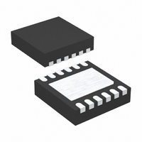
LT3498EDDB#TRPBF Linear Technology, LT3498EDDB#TRPBF Datasheet - Page 7

LT3498EDDB#TRPBF
Manufacturer Part Number
LT3498EDDB#TRPBF
Description
IC LED DRVR WT/OLED BCKLGT 12DFN
Manufacturer
Linear Technology
Type
Backlight, OLED, White LEDr
Datasheet
1.LT3498EDDBTRMPBF.pdf
(24 pages)
Specifications of LT3498EDDB#TRPBF
Topology
PWM, Step-Up (Boost)
Number Of Outputs
1
Internal Driver
Yes
Type - Primary
Backlight
Type - Secondary
OLED, White LED
Frequency
1.8MHz ~ 2.8MHz
Voltage - Supply
2.5 V ~ 12 V
Voltage - Output
32V
Mounting Type
Surface Mount
Package / Case
12-DFN
Operating Temperature
-40°C ~ 85°C
Current - Output / Channel
20mA
Internal Switch(s)
Yes
Lead Free Status / RoHS Status
Lead free / RoHS Compliant
Efficiency
-
Available stocks
Company
Part Number
Manufacturer
Quantity
Price
BLOCK DIAGRAM
PIN FUNCTIONS
V
Place a bypass capacitor from this pin to GND. See the
Applications Information section.
CAP2 (Pin 8): Output of the OLED Driver. This pin is
connected to the cathode of the internal Schottky diode.
Place a bypass capacitor from this pin to GND.
SW2 (Pin 9): Switch Pin. This is the collector of the in-
ternal NPN power switch. Minimize the metal trace area
connected to this pin to minimize EMI.
V
passed.
10μF
C3
OUT2
IN
2.21MΩ
R
FB2
(Pin 10): Input Supply Pin. Must be locally by-
C2
0.47μF
(Pin 7): Drain of Output Disconnect PMOS.
8
7
CAP2
V
OUT2
DISCONNECT
CONTROL
CONTROL
SHUNT
Q2
9
4
SW2
GND2
DRIVER
182kΩ
10μF
L2
A5
CONTROL
SWITCH
+
+
–
FB2
6
5
C
4.7μF
CTRL2
IN
START-UP
CONTROL
VREF
10
V
IN
SW1 (Pin 11): Switch Pin. Connect the inductor of the
white LED driver at this pin. Minimize metal trace area at
this pin to minimize EMI.
CAP1 (Pin 12): Output of the White LED Driver. This pin is
connected to the cathode of the internal Schottky. Connect
the output capacitor to this pin and the sense resistor from
this pin to the LED1 pin.
Exposed Pad (Pin 13): Ground. The Exposed Pad must
be soldered to the PCB.
GENERATOR
OSCILLATOR
–
+
2.3MHz
RAMP
∑
A2
COMPARATOR
R
C
C
15μF
C
L1
R
A1
S
–
+
+
Q
CTRL1 GND1
DRIVER
A3
2
+
–
SW1
11
3
Q1
R
OVERVOLTAGE
PROTECTION
A4
+
–
CAP1
LED1
LT3498
3498 BD
12
1
R
10Ω
SENSE1
1μF
C1
3498fa
7


