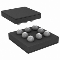
LM3501TLX-21/NOPB National Semiconductor, LM3501TLX-21/NOPB Datasheet - Page 12

LM3501TLX-21/NOPB
Manufacturer Part Number
LM3501TLX-21/NOPB
Description
IC LED DRVR WHT BCKLT 8-USMD
Manufacturer
National Semiconductor
Type
Backlight, White LEDr
Datasheet
1.LM3501TL-21NOPB.pdf
(18 pages)
Specifications of LM3501TLX-21/NOPB
Topology
PWM, Step-Up (Boost)
Number Of Outputs
1
Internal Driver
Yes
Type - Primary
Backlight
Type - Secondary
White LED
Frequency
850kHz ~ 1.15MHz
Voltage - Supply
2.7 V ~ 7 V
Voltage - Output
19.5 V ~ 20.5 V
Mounting Type
Surface Mount
Package / Case
8-MicroSMD
Operating Temperature
-40°C ~ 125°C
Current - Output / Channel
640mA
Internal Switch(s)
Yes
Efficiency
85%
Lead Free Status / RoHS Status
Lead free / RoHS Compliant
Other names
LM3501TLX-21
www.national.com
Operation
The LM3501 utilizes a synchronous Current Mode PWM
control scheme to regulate the feedback voltage over almost
all load conditions. The DC/DC controller acts as a controlled
current source ideal for white LED applications. The LM3501
is internally compensated preventing the use of any external
compensation components providing a compact overall so-
lution. The operation can best be understood referring to the
block diagram in Figure 2. At the start of each cycle, the
oscillator sets the driver logic and turns on the NMOS power
device conducting current through the inductor and turns off
the PMOS power device isolating the output from the V
pin. The LED current is supplied by the output capacitor
when the NMOS power device is active. During this cycle,
the output voltage of the EAMP controls the current through
the inductor. This voltage will increase for larger loads and
decrease for smaller loads limiting the peak current in the
inductor minimizing EMI radiation. The EAMP voltage is
compared with a voltage ramp and the sensed switch volt-
age. Once this voltage reaches the EAMP output voltage,
the PWM COMP will then reset the logic turning off the
NMOS power device and turning on the PMOS power de-
vice. The inductor current then flows through the PMOS
power device to the white LED load and output capacitor.
The inductor current recharges the output capacitor and
supplies the current for the white LED branches. The oscil-
lator then sets the driver logic again repeating the process.
FIGURE 2. LM3501 Block Diagram
SW
12
The Duty Limit Comp is always operational preventing the
NMOS power switch from being on more than one cycle and
conducting large amounts of current.
The LM3501 has dedicated protection circuitry active during
normal operation to protect the IC and the external compo-
nents. The Thermal Shutdown circuitry turns off both the
NMOS and PMOS power devices when the die temperature
reaches excessive levels. The LM3501 has a UVP Comp
that disables both the NMOS and PMOS power devices
when battery voltages are too low preventing an on state of
the power devices which could conduct large amounts of
current. The OVP Comp prevents the output voltage from
increasing beyond 15.5V (LM3501-16) and 20.5V (LM3501-
21) when the primary white LED network is removed or if
there is an LED failure, allowing the use of small (16V for
LM3501-16 and 25V for LM3501-21) ceramic capacitors at
the output. This comparator has hysteresis that will regulate
the output voltage between 15.5V and 14.6V typically for the
LM3501-16, and between 20.5V and 19.5V for the LM3501-
21. The LM3501 features a shutdown mode that reduces the
supply current to 0.1 uA and isolates the input and output of
the converter. The CNTRL pin can be used to change the
white LED current. A CNTRL voltage above 125 mV will
enable power to the LEDs and a voltage lower than 75 mV
will turn off the power to the LEDs.
20065304


