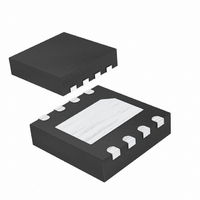
MAX1599ETA+T Maxim Integrated Products, MAX1599ETA+T Datasheet - Page 2

MAX1599ETA+T
Manufacturer Part Number
MAX1599ETA+T
Description
IC LED DRIVR WHITE BCKLGT 8-TDFN
Manufacturer
Maxim Integrated Products
Type
Backlight, White LEDr
Datasheet
1.MAX1561ETAT.pdf
(10 pages)
Specifications of MAX1599ETA+T
Constant Current
Yes
Topology
PWM, Step-Up (Boost)
Number Of Outputs
1
Internal Driver
Yes
Type - Primary
Backlight
Type - Secondary
White LED
Frequency
400kHz ~ 600kHz
Voltage - Supply
2.6 V ~ 5.5 V
Voltage - Output
26V
Mounting Type
Surface Mount
Package / Case
8-TDFN Exposed Pad
Operating Temperature
-40°C ~ 85°C
Current - Output / Channel
700mA
Internal Switch(s)
Yes
Efficiency
87%
Number Of Segments
6
Operating Supply Voltage
2.6 V to 5.5 V
Maximum Power Dissipation
1950 mW
Maximum Operating Temperature
+ 85 C
Mounting Style
SMD/SMT
Minimum Operating Temperature
- 40 C
Lead Free Status / RoHS Status
Lead free / RoHS Compliant
ABSOLUTE MAXIMUM RATINGS
IN to GND .................................................................-0.3V to +6V
PGND to GND .......................................................-0.3V to +0.3V
LX, OUT to GND .....................................................-0.3V to +30V
CTRL to GND...................-0.3V to the lower of +6V or (V
COMP, CS to GND.........................................-0.3 to (V
I
High-Efficiency, 26V Step-Up Converters
for Two to Six White LEDs
ELECTRICAL CHARACTERISTICS
(V
wise noted. Typical values are at T
Stresses beyond those listed under “Absolute Maximum Ratings” may cause permanent damage to the device. These are stress ratings only, and functional
operation of the device at these or any other conditions beyond those indicated in the operational sections of the specifications is not implied. Exposure to
absolute maximum rating conditions for extended periods may affect device reliability.
2
LX
Supply Voltage
UVLO Threshold
UVLO Hysteresis
Quiescent Current
Shutdown Supply Current
OVLO Threshold
OVLO Hysteresis
OUT Input Bias Current
Output Voltage Range
ERROR AMPLIFIER
CTRL to CS Regulation
CS Input Bias Current
CTRL Input Resistance
CTRL Dual-Mode Threshold
CTRL Dual-Mode Hysteresis
CTRL Shutdown Enable Delay
CS-to-COMP Transconductance
OSCILLATOR
Operating Frequency
Minimum Duty Cycle
Maximum Duty Cycle
IN
.............................................................................................1A
_______________________________________________________________________________________
= 3V, V
PARAMETER
OUT
= 20V, C
OUT
= 0.1µF, C
A
= +25°C.)
V
V
V
(Note 2)
V
MAX1561
MAX1599
PWM mode
Pulse skipping
CTRL = IN, CS = GND
V
No switching
CTRL = GND, V
V
V
V
(Note 1)
CTRL
CS
CTRL
COMP
IN
OUT
OUT
OUT
rising or falling
= V
COMP
rising
= 26V, V
= V
= 1V, V
= 1.0V
CTRL
1.0V
IN
= 0.15µF, R
, CTRL = GND
/10
IN
CTRL
OUT
= 2.6V to 5.5V
IN
IN
+ 0.3V)
> 0.24V
= V
+ 2V)
CONDITIONS
SENSE
IN
= 7.5Ω, V
Continuous Power Dissipation (T
Operating Temperature Range ...........................-40°C to +85°C
Junction Temperature ......................................................+150°C
Storage Temperature Range .............................-65°C to +150°C
Lead Temperature (soldering, 10s) .................................+300°C
3mm x 3mm 8-Pin TDFN
(derate 24.4mW/°C above +70°C) .............................1950mW
T
T
T
T
MAX1561
MAX1599
A
A
A
A
CTRL
= +25 C
= +85 C
= +25 C
= +85 C
= 1.5V, Figure 1, T
(V
0.095
2.10
13.6
0.80
MIN
IN
290
100
2.6
6.5
0.4
26
10
32
91
- V
A
A
D1
= 0°C to +85°C, unless other-
= +70°C)
)
0.100
TYP
2.38
0.38
0.01
0.01
0.03
16.4
500
170
0.3
8.2
1.0
0.5
40
27
20
50
12
94
1
2
5
0
0.105
MAX
2.55
0.55
25.5
10.5
21.0
1.25
780
240
5.5
0.6
29
30
82
2
1
1
UNITS
MHz
mV
mA
mV
mV
ms
µA
µA
µA
k
µS
%
%
V
V
V
V
V
V


