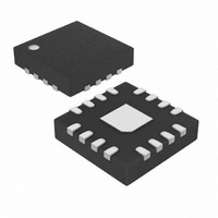
MAX8822ETE+ Maxim Integrated Products, MAX8822ETE+ Datasheet - Page 7

MAX8822ETE+
Manufacturer Part Number
MAX8822ETE+
Description
IC LED DRVR WHITE BCKLGT 16-TQFN
Manufacturer
Maxim Integrated Products
Type
Backlight, White LEDr
Datasheet
1.MAX8822ETE.pdf
(15 pages)
Specifications of MAX8822ETE+
Constant Current
Yes
Topology
Linear (LDO), PWM, Switched Capacitor (Charge Pump)
Number Of Outputs
4
Internal Driver
Yes
Type - Primary
Backlight
Type - Secondary
White LED
Frequency
1MHz
Voltage - Supply
2.7 V ~ 5.5 V
Voltage - Output
5V
Mounting Type
Surface Mount
Package / Case
16-TQFN Exposed Pad
Operating Temperature
-40°C ~ 85°C
Current - Output / Channel
24mA
Internal Switch(s)
Yes
Lead Free Status / RoHS Status
Lead free / RoHS Compliant
Efficiency
-
Lead Free Status / Rohs Status
Details
Driver with Dual LDOs in 3mm x 3mm Thin QFN
8–11
PIN
12
13
14
15
16
—
1
2
3
4
5
6
7
Ultra-Efficient Negative Charge-Pump LED
LED4–LED1
ENLDO
ENLED
NAME
LDO1
LDO2
GND
NEG
C2N
C1N
C1P
C2P
REF
EP
IN
_______________________________________________________________________________________
Supply Voltage Input. Bypass IN to GND with a 4.7µF ceramic capacitor placed as close as possible
to the IC. The input voltage range is 2.7V to 5.5V.
Ground. Connect to system ground. GND is used for charge-pump switching currents.
Transfer Capacitor 1 Positive Connection. Connect a 1µF ceramic capacitor from C1P to C1N.
Transfer Capacitor 2 Positive Connection. Connect a 1µF ceramic capacitor from C2P to C2N.
Transfer Capacitor 2 Negative Connection. Connect a 1µF ceramic capacitor from C2P to C2N.
Transfer Capacitor 1 Negative Connection. Connect a 1µF ceramic capacitor from C1P to C1N.
Charge-Pump Output. Bypass NEG to GND with a 2.2µF ceramic capacitor placed as close as
possible to the IC.
LED Current Regulators. Connect LED_ to the cathodes of the external LEDs. LED_ is high
impedance in shutdown. Connect any unused LED_ to IN to disable the corresponding current
regulator. LED_ current is programmed by pulsing ENLED as described in the LED Dimming Control
section.
LD O1 Outp ut. Byp ass LD O 1 to GN D w i th a 1µF cer am i c cap aci tor p l aced as cl ose as p ossi b l e to the IC .
The LD O 1 and LD O2 outp ut vol tag e com b i nati on i s sel ected b y p ul si ng E N LD O l ow . S ee the LD O1/LD O2
Outp ut V ol tag e C ontr ol secti on.
LD O2 Outp ut. Byp ass LD O 2 to GN D w i th a 1µF cer am i c cap aci tor p l aced as cl ose as p ossi b l e to the IC .
The LD O 1 and LD O2 outp ut vol tag e com b i nati on i s sel ected b y p ul si ng E N LD O l ow . S ee the LD O1/LD O2
Outp ut V ol tag e C ontr ol secti on.
WLED Enable and Dimming Control Input. Pulse ENLED low to program LED_ current. Hold ENLED
low for at least 2.5ms to place the LED drivers in shutdown. See the LED Dimming Control section.
LDO Enable and Voltage Control Input. Pulse ENLDO low to program the output voltage of both
LDO1 and LDO2 to one of sixteen different combinations. Hold ENLDO low for at least 2.5ms to
place the LDOs in shutdown. See the LDO1/LDO2 Output Voltage Control section.
Refer ence. Byp ass RE F to GN D w i th a 0.1µF cer am i c cap aci tor p l aced as cl ose as p ossi b l e to the IC .
V
Exposed Paddle. Connect EP to GND. For good thermal dissipation, solder the exposed paddle to
the power ground plane.
R E F
r eg ul ates to 1.2V ( typ ) .
FUNCTION
Pin Description
7


