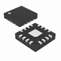
MAX6965ATE+T Maxim Integrated Products, MAX6965ATE+T Datasheet - Page 9

MAX6965ATE+T
Manufacturer Part Number
MAX6965ATE+T
Description
IC LED DRIVER LINEAR 16-TQFN
Manufacturer
Maxim Integrated Products
Type
Linear (I²C Interface)r
Datasheet
1.MAX6965AEE.pdf
(22 pages)
Specifications of MAX6965ATE+T
Topology
Open Drain, PWM
Number Of Outputs
9
Internal Driver
Yes
Type - Primary
Backlight, LED Blinker
Type - Secondary
RGB, White LED
Frequency
400kHz
Voltage - Supply
2 V ~ 3.6 V
Voltage - Output
7V
Mounting Type
Surface Mount
Package / Case
16-TQFN Exposed Pad
Operating Temperature
-40°C ~ 125°C
Current - Output / Channel
50mA
Internal Switch(s)
Yes
Number Of Segments
6
Operating Supply Voltage
2 V to 3.6 V
Maximum Supply Current
110 uA
Maximum Power Dissipation
1176 mW
Maximum Operating Temperature
+ 125 C
Mounting Style
SMD/SMT
Minimum Operating Temperature
- 40 C
Lead Free Status / RoHS Status
Lead free / RoHS Compliant
Efficiency
-
Lead Free Status / Rohs Status
Details
The MAX6965 is read using the MAX6965’s internally
stored command byte as an address pointer the same
way the stored command byte is used as an address
pointer for a write. The pointer autoincrements after
each data byte is read using the same rules as for a
write (Table 2). Thus, a read is initiated by first configur-
ing the MAX6965’s command byte by performing a
Figure 7. Command Byte Received
Figure 8. Command and Single Data Byte Received
Figure 9. n Data Bytes Received
Figure 10. Write Timing Diagram
O7–O0
WRITE TO OUTPUT PORTS REGISTERS (BLINK PHASE 0 REGISTERS/BLINK PHASE 1 REGISTERS)
SCL
SDA
S
S
S A6 A5 A4 A3 A2 A1 A0
START CONDITION
HOW COMMAND BYTE AND DATA BYTE MAP INTO
HOW COMMAND BYTE AND DATA BYTE MAP INTO
1
SLAVE ADDRESS
2
9-Output LED Driver with Intensity Control
S
3
_______________________________________________________________________________________
4
ACKNOWLEDGE FROM
ACKNOWLEDGE FROM MAX6965
SLAVE ADDRESS
SLAVE ADDRESS
5
6
Message Format for Reading
MAX6965's REGISTERS
MAX6965's REGISTERS
7
COMMAND BYTE IS STORED ON RECEIPT OF
R/W
0
8
SLAVE ADDRESS
9
R/W
R/W
A
ACKNOWLEDGE FROM SLAVE
MAX6965
COMMAND BYTE
ACKNOWLEDGE FROM MAX6965
0
0
0
0
0
A
A
0
D15 D14 D13 D12 D11 D10
D15 D14 D13 D12 D11 D10
STOP CONDITION
0
R/W
and Hot-Insertion Protection
0
0
0
ACKNOWLEDGE FROM
ACKNOWLEDGE FROM MAX6965
COMMAND BYTE
COMMAND BYTE
1
A
A
ACKNOWLEDGE FROM SLAVE
MSB
D15
write (Figure 7). The master can now read n consecu-
tive bytes from the MAX6965 with the first data byte
being read from the register addressed by the initial-
ized command byte. When performing read-after-write
verification, remember to reset the command byte’s
address because the stored command byte address
has been autoincremented after the write (Table 2).
D14
D9
D9
DATA1
MAX6965
D8
D13
D8
A
A
D12
COMMAND BYTE
ACKNOWLEDGE FROM MAX6965
LSB
D7
D7
D11
AUTOINCREMENT MEMORY ADDRESS
AUTOINCREMENT MEMORY ADDRESS
D6
D6
A
ACKNOWLEDGE FROM SLAVE
MSB
D10
D5
D5
ACKNOWLEDGE FROM
ACKNOWLEDGE FROM MAX6965
t
DV
DATA BYTE
DATA BYTE
D4
D4
D9
BYTES
BYTE
DATA1 VALID
N
1
DATA2
D3
D3
D8
D2
D2
A
t
D1
D1
DV
MAX6965
LSB
P
D0
D0
CONDITION
A
STOP
DATA2 VALID
A
A
P
P
P
9


