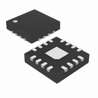
MAX1986ETE+T Maxim Integrated Products, MAX1986ETE+T Datasheet - Page 15

MAX1986ETE+T
Manufacturer Part Number
MAX1986ETE+T
Description
IC LED DRVR WHITE BCKLGT 16-TQFN
Manufacturer
Maxim Integrated Products
Type
Backlight, White LEDr
Datasheet
1.MAX1986ETET.pdf
(17 pages)
Specifications of MAX1986ETE+T
Topology
PWM, Step-Up (Boost)
Number Of Outputs
4
Internal Driver
Yes
Type - Primary
Backlight
Type - Secondary
White LED
Frequency
800kHz ~ 1.2MHz
Voltage - Supply
2.7 V ~ 5.5 V
Mounting Type
Surface Mount
Package / Case
16-TQFN Exposed Pad
Operating Temperature
-40°C ~ 85°C
Current - Output / Channel
25mA
Internal Switch(s)
Yes
Efficiency
90%
Lead Free Status / RoHS Status
Lead free / RoHS Compliant
Voltage - Output
-
Lead Free Status / Rohs Status
Details
The input capacitor reduces the current peaks drawn
from the input supply and reduces noise injection into
all devices running from that supply. The input voltage
source impedance determines the required size of the
input capacitor. The standard application circuits
(Figures 1, 6, and 7) use an input capacitor equal to the
output capacitor to accommodate the high impedance
seen in a typical lab environment. Actual applications
usually have much lower source impedance since the
step-up regulator typically runs directly from a low-
impedance battery. Often, the input capacitor can be
reduced by 50% or more of the output capacitor value.
To prevent noise from coupling into the device, connect
an additional 0.1µF ceramic capacitor from the IN pin to
the GND pin. Place that capacitor within 5mm of the pins.
The full-scale current through each LED can be set
using SETI. When SETI is connected to IN, the full-scale
LED current is set to the default value of 18mA. When
SETI is connected to GND, the LED current is set to
0.5mA LED test mode. If SETI is connected with a resis-
tor to GND, the full-scale LED current can be adjusted
from 14mA to 25mA:
where K = 3851, and V
voltage.
I
LED FS
Setting the Maximum LED Current
(
)
=
______________________________________________________________________________________
12
mA K
Input Capacitor Selection
REF
+
×
is the internal reference
0 75
.
R
SETI
×
V
REF
Ultra-High-Efficiency White
Careful PC board layout is very important for proper
operation. Use the following guidelines for good PC
board layout:
1) Minimize the area of high-current loops by placing
2) Create islands for the analog ground and power
3) Maximize the width of the power ground traces to
4) Place the IN pin and REF pin bypass capacitors
5) Minimize the size of LX node while keeping it wide
Refer to the MAX1985 evaluation kit for an example of
proper board layout.
TRANSISTOR COUNT: 3016
the input capacitors, inductor, and output capaci-
tors less than 0.2in (5mm) from the LX and GND
pins. Connect these components with wide traces.
Avoid using vias in the high-current paths. If vias
are unavoidable, use many vias in parallel to
reduce resistance and inductance.
ground. The analog ground island includes the
exposed backside pad of the device, the REF
bypass capacitor ground, and the SETI resistor
ground. The power ground island includes the GND
pin, the common ground for the current regulators
(LDG), and the step-up regulator’s input/output
capacitor grounds. The analog ground and power
ground islands are connected together at only one
location using a short trace between the GND pin
and the exposed backside pad underneath the
device.
improve efficiency, and reduce output-voltage rip-
ple and noise spikes.
within 5mm to the device.
and short to reduce radiated EMI.
PC Board Layout and Grounding
LED Drivers
Chip Information
15


