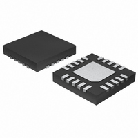
MAX16805ATP+ Maxim Integrated Products, MAX16805ATP+ Datasheet - Page 12

MAX16805ATP+
Manufacturer Part Number
MAX16805ATP+
Description
IC LED DRIVR HIGH BRIGHT 20-TQFN
Manufacturer
Maxim Integrated Products
Type
HBLED Driverr
Datasheet
1.MAX16805ATP.pdf
(19 pages)
Specifications of MAX16805ATP+
Constant Current
Yes
Topology
PWM
Number Of Outputs
1
Internal Driver
Yes
Type - Primary
Automotive
Type - Secondary
High Brightness LED (HBLED)
Frequency
400kHz
Voltage - Supply
5.5 V ~ 40 V
Voltage - Output
5.1V
Mounting Type
Surface Mount
Package / Case
20-TQFN Exposed Pad
Operating Temperature
-40°C ~ 125°C
Current - Output / Channel
350mA
Internal Switch(s)
Yes
High Level Output Current
350 mA
Operating Supply Voltage
5.5 V to 40 V
Maximum Power Dissipation
2758.6 mW
Maximum Operating Temperature
+ 125 C
Mounting Style
SMD/SMT
Minimum Operating Temperature
- 40 C
Lead Free Status / RoHS Status
Lead free / RoHS Compliant
Efficiency
-
Lead Free Status / Rohs Status
Lead free / RoHS Compliant
EEPROM-Programmable, High-Voltage, 350mA
LED Drivers with LED Current Foldback
One data bit is transferred during each clock pulse.
The data on the SDA line must remain stable while SCL
is high
The acknowledge bit is a clocked 9th bit that the recipi-
ent uses to handshake receipt each byte of data
(Figure
requires 9 bits. The master controller generates the 9th
Figure
Figure 5. Acknowledge
Figure
12
SDA
SCL
SDA
SCL
______________________________________________________________________________________
SDA
START
SCL
4. Bit Transfer
6. Slave Address
(Figure
5). Therefore, each byte effectively transferred
DATA STABLE,
DATA VALID
4).
START
CHANGE OF DATA
MSB
A7
1
ALLOWED
2
A6
1
Acknowledge
Bit Transfer
3
A5
2
4
A4
clock pulse, and the recipient pulls down SDA during
the acknowledge clock pulse, so the SDA line remains
stable low during the high period of the clock pulse.
The MAX16805/MAX16806 have a 7-bit-long slave
address
bit slave address is the R/W bit. Set the R/W bit low for
a write command and high for a read command.
Table
5
A3
WRITE ADDRESS (HEX)
1. Slave Address
(Figure
6
A2
0xEE
NOT ACKNOWLEDGE
8
ACKNOWLEDGE
6,
Table
7
A1
1). The 8th bit following the 7-
8
RW
9
READ ADDRESS (HEX)
Slave Address
0xEF
ACK
9


