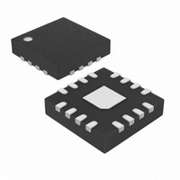
MAX6946ATE+T Maxim Integrated Products, MAX6946ATE+T Datasheet - Page 4

MAX6946ATE+T
Manufacturer Part Number
MAX6946ATE+T
Description
IC LED DRIVER LINEAR 16-TQFN
Manufacturer
Maxim Integrated Products
Type
Linear (I²C Interface)r
Datasheet
1.MAX6947ATE.pdf
(24 pages)
Specifications of MAX6946ATE+T
Constant Current
Yes
Topology
Open Drain, PWM
Number Of Outputs
10
Internal Driver
Yes
Type - Primary
Backlight
Type - Secondary
RGB, White LED
Frequency
400kHz
Voltage - Supply
2.25 V ~ 3.6 V
Voltage - Output
7V
Mounting Type
Surface Mount
Package / Case
16-TQFN Exposed Pad
Operating Temperature
-40°C ~ 125°C
Current - Output / Channel
20mA
Internal Switch(s)
Yes
Number Of Segments
3
Low Level Output Current
21.12 mA
Operating Supply Voltage
2.25 V to 3.6 V
Maximum Supply Current
60 uA
Maximum Power Dissipation
1176 mW
Maximum Operating Temperature
+ 125 C
Mounting Style
SMD/SMT
Minimum Operating Temperature
- 40 C
Lead Free Status / RoHS Status
Lead free / RoHS Compliant
Efficiency
-
Lead Free Status / Rohs Status
Details
10-Port, Constant-Current LED Driver and
I/O Expander with PWM Intensity Control
TIMING CHARACTERISTICS (Figure 8)
(V
4
Note 1: All parameters are tested at T
Note 2: Port current is factory trimmed to meet a median sink current of 20mA and 10mA over all ports. The ΔI
Note 3: A master device must provide a hold time of at least 300ns for the SDA signal (referred to V
Note 4: Not production tested. Guaranteed by design.
Note 5: C
Note 6: I
Note 7: Guaranteed by design. Input filters on the SDA and SCL inputs suppress noise spikes of less than 50ns.
Internal PWM Clock Frequency
External PWM Clock Frequency
Serial-Clock Frequency
Bus Free Time Between a STOP and
a START Condition
Hold Time, (Repeated) START
Condition
Repeated START Condition Setup
Time
STOP Condition Setup Time
Data Hold Time
Data Setup Time
SCL Clock Low Period
SCL Clock High Period
Rise Time of Both SDA and SCL
Signals, Receiving
Fall Time of Both SDA and SCL
Signals, Receiving
Fall Time of SDA Transmitting
Pulse Width of Spike Supressed
Capacitive Load for Each Bus Line
RST Pulse Width
RST Rising Edge to
MAX6946/MAX6947 ACK to Cancel
Reset Run
RST Rising Edge to
MAX6946/MAX6947 ACK to Ensure
Reset Run
DD
_______________________________________________________________________________________
= 2.25V to 3.6V, T
guarantees current matching between parts.
bridge the undefined region of SCL’s falling edge.
SINK
b
= total capacitance of one bus line in picoFarads; t R and t F are measured between 0.3 x V
PARAMETER
≤ 6mA.
A
= T
MIN
to T
MAX
A
SYMBOL
= +25°C. Specifications over temperature are guaranteed by design.
, unless otherwise noted. Typical values are at V
t
t
t
t
t
t
t
HD, STA
SU, STO
HD, DAT
SU, DAT
RSTRUN
RSTRUN
SU, STA
t
t
t
f
f
t
HIGH
f
LOW
F, TX
OSC
SCL
BUF
t
C
INT
t
t
t
SP
W
R
F
b
16-pin TQFN
16-bump WLP
(Note 3)
(Notes 4, 5)
(Notes 4, 5)
(Notes 4, 6)
(Note 7)
(Note 4)
Reset Run enabled,
internal oscillator
enabled
Reset Run enabled, internal oscillator
enabled
CONDITIONS
16-pin TQFN
16-bump WLP
DD
= 3.3V, T
MIN
180
1.3
0.6
0.6
0.6
1.3
0.7
0.1
5.6
23
20
IL
A
of the SCL signal) in order to
DD
= +25°C.) (Note 1)
+ 0.1C
+ 0.1C
+ 0.1C
and 0.7 x V
TYP
32
32
20
20
20
50
OUT
b
b
b
specification
MAX
DD
100
400
300
300
250
400
0.9
3.0
2.5
42
45
.
UNITS
kHz
kHz
kHz
ms
ms
µs
µs
µs
µs
µs
µs
pF
µs
µs
ns
ns
ns
ns
ns


