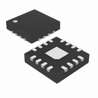
MAX6967ATE+ Maxim Integrated Products, MAX6967ATE+ Datasheet - Page 23

MAX6967ATE+
Manufacturer Part Number
MAX6967ATE+
Description
IC LED DRIVER LINEAR 16-TQFN
Manufacturer
Maxim Integrated Products
Type
Linear (Serial Interface)r
Datasheet
1.MAX6966ATE.pdf
(29 pages)
Specifications of MAX6967ATE+
Constant Current
Yes
Topology
Open Drain, PWM
Number Of Outputs
10
Internal Driver
Yes
Type - Primary
Backlight
Type - Secondary
RGB, White LED
Frequency
270kHz ~ 450kHz
Voltage - Supply
2.25 V ~ 3.6 V
Voltage - Output
7V
Mounting Type
Surface Mount
Package / Case
16-TQFN Exposed Pad
Operating Temperature
-40°C ~ 125°C
Current - Output / Channel
20mA
Internal Switch(s)
Yes
Number Of Segments
10
Low Level Output Current
21.1 mA
Operating Supply Voltage
2.25 V to 3.6 V
Maximum Supply Current
730 uA
Maximum Power Dissipation
1176 mW
Maximum Operating Temperature
+ 125 C
Mounting Style
SMD/SMT
Minimum Operating Temperature
- 40 C
Lead Free Status / RoHS Status
Lead free / RoHS Compliant
Efficiency
-
Lead Free Status / Rohs Status
Details
The MAX6966/MAX6967 are written to using the follow-
ing sequence
1) Take SCLK low.
2) Take CS low. This enables the internal 16-bit shift reg-
3) Clock 16 bits of data into DIN, D15 first to D0 last,
4) Take CS high (either while SCLK is still high after
5) Take SCLK low (if not already low).
If fewer or greater than 16 bits are clocked into the
MAX6966/MAX6967 between taking CS low and taking
CS high again, the MAX6966/MAX6967 store the last 16
bits received, including the previous transmission(s).
The general case is when n bits (where n > 16) are
transmitted to the MAX6966/MAX6967. The last bits
comprising bits {n-15} to {n}, are retained, and are par-
allel loaded into the 16-bit latch as bits D15 to D0,
respectively
Figure
Figure
DOUT
SCLK
DOUT
ister.
observing the setup and hold times. Bit D15 is low,
indicating a write command.
clocking in the last data bit, or after taking SCLK
low).
SCLK
DIN
CS
DIN
CS
11. 16-Bit Write Transmission to the MAX6966/MAX6967
12. Transmission of More than 16 Bits to the MAX6966/MAX6967
10-Port Constant-Current LED Drivers and I/O
(Figure
BIT
1
D15
= 0
(Figure
BIT
2
______________________________________________________________________________________
D14
12).
11):
Expanders with PWM Intensity Control
N-15
N-31
D13
N-14
N-30
D12
N-13
N-29
D11
N-28
N-12
D10
N-11
N-27
D9
N-10
N-26
D8
N-25
N-9
N-8
N-24
Any register data within the MAX6966/MAX6967 can be
read by sending a logic high to bit D15. The sequence is:
1) Take SCLK low.
2) Take CS low. This enables the internal 16-bit shift
3) Clock 16 bits of data into DIN, D15 first to D0 last.
4) Take CS high (either while SCLK is still high after
5) Take SCLK low (if not already low).
6) Issue another read or write command, and examine
D7
register.
D15 is high, indicating a read command and bits
D14 through D8 contain the address of the register
to read. Bits D7 to D0 contain dummy data, which is
discarded.
clocking in the last data bit, or after taking SCLK
low). Positions D7 through D0 in the shift register are
now loaded with the register data addressed by bits
D15 through D8.
the bit stream at DOUT; the second 8 bits are the
contents of the register addressed by bits D14
through D8 in step 3).
.
N-23
N-7
D6
.
N-22
N-6
D5
N-21
N-5
D4
N-20
N-4
Reading Device Registers
D3
N-19
N-3
D2
N-18
N-2
D1
N-17
N-1
N-16
N
D0
D15 = 0
23


