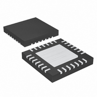
MAX16821AATI+ Maxim Integrated Products, MAX16821AATI+ Datasheet - Page 7

MAX16821AATI+
Manufacturer Part Number
MAX16821AATI+
Description
IC LED DRIVR HIGH BRIGHT 28-TQFN
Manufacturer
Maxim Integrated Products
Type
HBLED Driverr
Datasheet
1.MAX16821BATI.pdf
(24 pages)
Specifications of MAX16821AATI+
Topology
High Side, Low Side, PWM, SEPIC, Step-Down (Buck), Step-Up (Boost)
Number Of Outputs
1
Internal Driver
No
Type - Primary
Automotive, Backlight
Type - Secondary
High Brightness LED (HBLED)
Frequency
125kHz ~ 1.5MHz
Voltage - Supply
4.75 V ~ 5.5 V, 7 V ~ 28 V
Voltage - Output
5.1V
Mounting Type
Surface Mount
Package / Case
28-TQFN Exposed Pad
Operating Temperature
-40°C ~ 125°C
Current - Output / Channel
30A
Internal Switch(s)
Yes
Low Level Output Current
4000000 uA (Typ)
High Level Output Current
4000000 uA (Typ)
Operating Supply Voltage
7 V to 28 V
Maximum Supply Current
5.5 mA
Maximum Power Dissipation
2758 mW
Maximum Operating Temperature
+ 125 C
Mounting Style
SMD/SMT
Minimum Operating Temperature
- 40 C
Lead Free Status / RoHS Status
Lead free / RoHS Compliant
Efficiency
-
Lead Free Status / Rohs Status
Lead free / RoHS Compliant
8, 22, 25
PIN
2, 7
10
11
12
13
14
15
16
17
18
19
20
21
23
24
26
27
28
—
1
3
4
5
6
9
RT/SYNC
CLKOUT
SENSE+
SENSE-
EAOUT
NAME
MODE
PGND
SGND
OUTV
DIFF
CSN
N.C.
CLP
EAN
CSP
BST
V
V
I.C.
OVI
DH
DL
EN
LX
EP
IN
CC
DD
_______________________________________________________________________________________
Power-Supply Ground
No Connection. Not internally connected.
Low-Side Gate-Driver Output
Boost-Flying Capacitor Connection. Reservoir capacitor connection for the high-side MOSFET driver
supply. Connect a ceramic capacitor between BST and LX.
High-Side MOSFET Source Connection
High-Side Gate-Driver Output
Signal Ground. SGND is the ground connection for the internal control circuitry. Connect SGND and PGND
together at one point near the IC.
Oscillator Output. If MODE is low, the rising edge of CLKOUT phase shifts from the rising edge of DH by
180°. If MODE is high, the rising edge of CLKOUT phase shifts from the rising edge of DL by 180°.
Buck/Boost Mode Selection Input. Drive MODE low for low-side buck mode operation. Drive MODE high for
boost or high-side buck mode operation. MODE has an internal 5µA pulldown current to ground.
Output Enable. Drives EN high or leave unconnected for normal operation. Drive EN low to shut down the
power drivers. EN has an internal 15µA pullup current.
Switching Frequency Programming. Connect a resistor from RT/SYNC to SGND to set the internal oscillator
frequency. Drive RT/SYNC to synchronize the switching frequency with an external clock.
Inductor Current-Sense Output. OUTV is an amplifier output voltage proportional to the inductor current.
The voltage at OUTV = 135 x (V
Internally Connected. Connect to SGND for proper operation.
Overvoltage Protection. When OVI exceeds the programmed output voltage by 12.7%, the low-side and
the high-side drivers are turned off. When OVI falls 20% below the programmed output voltage, the drivers
are turned on after power-on reset and soft-start cycles are completed.
Current-Error-Amplifier Output. Compensate the current loop by connecting an RC network to ground.
Voltage-Error-Amplifier Output. Connect EAOUT to the external gain-setting network.
Voltage-Error-Amplifier Inverting Input
Differential Remote-Sense Amplifier Output. DIFF is the output of a precision amplifier with SENSE+ and
SENSE- as inputs.
Current-Sense Differential Amplifier Negative Input. The differential voltage between CSN and CSP is
amplified internally by the current-sense amplifier (Gain = 34.5) to measure the inductor current.
Current-Sense Differential Amplifier Positive Input. The differential voltage between CSP and CSN is
amplified internally by the current-sense amplifier (Gain = 34.5) to measure the inductor current.
Differential LED Current-Sensing Negative Input. Connect SENSE- to the negative side of the LED current-
sense resistor or to the negative feedback point.
Differential LED Current-Sensing Positive Input. Connect SENSE+ to the positive side of the LED current-
sense resistor, or to the positive feedback point.
Supply Voltage Input. Connect IN to V
Internal +5V Regulator Output. V
ceramic capacitors.
Low-Side Driver Supply Voltage
Exposed Pad. EP is internally connected to SGND. Connect EP to a large-area ground plane for effective
power dissipation. Connect EP to SGND. Do not use as a ground connection.
Drivers with Rapid Current Pulsing
High-Power Synchronous HBLED
CSP
CC
- V
is derived from V
CC
CSN
, for a 4.75V to 5.5V input supply range.
).
FUNCTION
IN
. Bypass V
CC
to SGND with 4.7µF and 0.1µF
Pin Description
7


