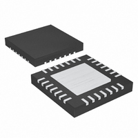
MAX8631XETI+T Maxim Integrated Products, MAX8631XETI+T Datasheet - Page 9

MAX8631XETI+T
Manufacturer Part Number
MAX8631XETI+T
Description
IC LED DRVR WHITE BCKLGT 28-TQFN
Manufacturer
Maxim Integrated Products
Type
Backlight, White LED (Serial Interface)r
Datasheet
1.MAX8631YETIT.pdf
(15 pages)
Specifications of MAX8631XETI+T
Constant Current
Yes
Topology
Linear (LDO), Switched Capacitor (Charge Pump)
Number Of Outputs
8
Internal Driver
Yes
Type - Primary
Backlight, Flash/Torch
Type - Secondary
White LED
Frequency
1MHz
Voltage - Supply
2.7 V ~ 5.5 V
Voltage - Output
5V
Mounting Type
Surface Mount
Package / Case
28-TQFN Exposed Pad
Operating Temperature
-40°C ~ 85°C
Current - Output / Channel
200mA
Internal Switch(s)
Yes
Efficiency
85%
Lead Free Status / RoHS Status
Lead free / RoHS Compliant
13–16
9–12
PIN
17
18
19
20
21
22
1
2
3
4
5
6
7
8
1x/1.5x/2x White LED Charge Pump with Two
ENLDO
M4–M1
REFBP
NAME
LDO1
LDO2
SETM
F4–F1
ENM2
ENM1
SETF
GND
C1N
ENF
PIN
_______________________________________________________________________________________
P2
IN
Supply Voltage Input. Bypass to PGND with a 10µF ceramic capacitor. The input voltage range is
2.7V to 5.5V. PIN is high impedance during shutdown.
Chip Supply Voltage Input. Bypass to GND with a 10µF ceramic capacitor as close to the IC as
possible. The input voltage range is 2.7V to 5.5V. IN is high impedance during shutdown.
Ground. Connect GND to system ground and the input bypass capacitor as close to the IC as
possible.
LDO1 Output. Bypass with a 1µF ceramic capacitor to GND. LDO1 is pulled to ground through an
internal 400kΩ during shutdown.
LDO2 Output. Bypass with a 1µF ceramic capacitor to GND. LDO2 is pulled to ground through an
internal 400kΩ during shutdown.
Reference Filter. Bypass REFBP with a 0.01µF ceramic capacitor to GND.
Bias Current Set Input for F1–F4. The current flowing out of SETF sets the maximum (100%) bias
current into each LED. V
GND to set the flash current. R
Bi as C ur r ent S et Inp ut for M 1–M 4. The cur r ent fl ow i ng out of S E TM sets the m axi m um ( 100%) b i as
cur r ent i nto each LE D . V
to set the m ai n LE D cur r ent. R
400m A C om b i ned C ur r ent Fl ash LE D C athod e C onnecti on and C har g e- P um p Feed b ack. C ur r ent fl ow i ng
i nto F_ i s b ased on I
i np ut for ces OU T to op er ate at ap p r oxi m atel y 5V . C onnect F_ to OU T i f thi s LE D i s not p op ul ated .
30mA M ai n LE D Cathod e Connecti on and C har g e- P ump Feed b ack. C ur rent fl owi ng i nto M _ i s based on the
E N _ confi g ur ation and I
any M _ for ces OU T to oper ate at ap pr oxim atel y 5V . Connect M_ to OU T i f thi s LE D i s not p op ul ated .
Default Output-Voltage Select Input. P1 and P2 set the LDO1 and LDO2 voltages to one of nine
combinations (Table 2). P2 is high impedance in an off condition and shortly after an on condition.
LDO Output Enable. Drive to a logic-level high to turn on both LDOs. Drive to a logic-level low to turn
off both LDOs.
Enable and Dimming Control for M1–M4. Drive both ENM1 and ENM2 to a logic-level high to turn on
the main LEDs. Drive both ENM1 and ENM2 to a logic-level low to turn off the main LEDs. The
dimming technique is discussed in the Applications Information section.
Enable and Dimming Control for M1–M4. Drive both ENM1 and ENM2 to a logic-level high to turn on
the main LEDs. Drive both ENM1 and ENM2 to a logic-level low to turn off the main LEDs. The
dimming technique is discussed in the Applications Information section.
Enable and Dimming Control for F1–F4. Drive ENF to a logic-level high to turn on the flash LEDs.
Drive ENF to a logic-level low to turn off the flash LEDs. The dimming technique is discussed in the
Applications Information section.
Transfer Capacitor 1 Negative Connection. Connect a 1µF ceramic capacitor between C1P and C1N.
C1N is internally shorted to IN during shutdown.
LDOs in 4mm x 4mm Thin QFN
S E T F
S E TM
. The char g e p um p r eg ul ates the l ow est F_ vol tag e to 0.15V . Gr ound i ng any F_
S E T M
SETF
. The char ge p um p reg ulates the l owest M _ inp ut voltag e to 0.15V . Gr ound i ng
S E T M
i s i nter nal l y b i ased to 0.6V . C onnect a r esi stor ( R
is internally biased to 0.6V. Connect a resistor (R
SETF
= 138 / I
= 414 / I
L E D ( M AX )
LED(MAX)
FUNCTION
. S E TM i s hi g h i m p ed ance d ur i ng shutd ow n.
. SETF is high impedance during shutdown.
Pin Description
S E T M
SETF
) fr om S E TM to GN D
) from SETF to
9


