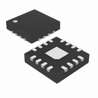
MAX1570ETE+ Maxim Integrated Products, MAX1570ETE+ Datasheet - Page 9

MAX1570ETE+
Manufacturer Part Number
MAX1570ETE+
Description
IC LED DRVR WHITE BCKLGT 16-TQFN
Manufacturer
Maxim Integrated Products
Type
Backlight, White LEDr
Datasheet
1.MAX1570ETET.pdf
(11 pages)
Specifications of MAX1570ETE+
Constant Current
Yes
Topology
PWM, Step-Down (Buck), Step-Up (Boost), Switched Capacitor (Charge Pump)
Number Of Outputs
5
Internal Driver
Yes
Type - Primary
Backlight
Type - Secondary
White LED
Frequency
1MHz
Voltage - Supply
2.7 V ~ 5.5 V
Mounting Type
Surface Mount
Package / Case
16-TQFN Exposed Pad
Operating Temperature
-40°C ~ 85°C
Current - Output / Channel
30mA
Internal Switch(s)
Yes
Number Of Segments
5
Low Level Output Current
30 mA
Operating Supply Voltage
2.7 V to 5.5 V
Maximum Supply Current
3.5 mA
Maximum Power Dissipation
1349 mW
Maximum Operating Temperature
+ 85 C
Mounting Style
SMD/SMT
Minimum Operating Temperature
- 40 C
Lead Free Status / RoHS Status
Lead free / RoHS Compliant
Voltage - Output
-
Efficiency
-
Lead Free Status / Rohs Status
Details
For LED drivers, input ripple is more important than out-
put ripple. Input ripple depends on the source supply’s
impedance. Adding a lowpass filter to the input further
reduces input ripple. Figure 3 shows a C-R-C filter used
to reduce input ripple to less than 2mV
a 75mA load. Alternately, increasing C
4.7µF yields input ripple of 17mV
tively, with only a small increase in footprint. The 1x
mode has very low input ripple.
The MAX1570 is a high-frequency switched-capacitor
voltage regulator. For best circuit performance, use a
solid ground plane and place C
to the MAX1570 as possible. Also, place their ground
tails close together. Connect PGND and GND directly
under the IC to the exposed paddle, and connect C
and C
supply connections should be short; if this is not possi-
ble, an additional input supply filter capacitor (tantalum
or electrolytic) may be required. Refer to the MAX1570
EV kit for a good layout example.
Figure 1. Dimming Using PWM Signal into EN1
PWM INPUT
V
IN
R SET
OUT
1µF
as close as possible to PGND. The input
EN2
EN1
SET
IN
White LED Current Regulator with 1x/1.5x
C1P
PC Board Layout and Routing
1µF
_______________________________________________________________________________________
GND
MAX1570
C1N
C2P
PGND
1µF
P-P
IN
C2N
OUT
LED1
LED2
LED3
LED4
LED5
and C
or 9mV
4.7µF
P-P
Input Ripple
IN
OUT
when driving
P-P
to 2.2µF or
High-Efficiency Charge Pump
, respec-
as close
IN
Typical external component values are shown in Table
2 and Table 3.
Maximum power dissipation occurs around 4.2V on IN
and 4.0V at OUT with maximum load current.
At higher IN voltages this device switches to 1x mode
and power dissipation is lowered.
Figure 2. Dimming Using Filtered-PWM Signal
Figure 3. C-R-C Filter Reduces Input Ripple
TRANSISTOR COUNT: 3187
P
V
PWM INPUT
D
IN
0 TO 25V
=
[
2.2µF
(
(
1 5
R SET
1Ω
14.3kΩ
.
R1
1µF
×
C3
V
2.2µF
V
IN
IN
EN1
EN2
SET
14.3kΩ
IN
9.09kΩ
R2
)
R
1µF
SET
−
C1P
1µF
V
EN1
EN2
SET
OUT
IN
GND
MAX1570
C1N
C1P
)
1µF
+
Component Selection
Chip Information
MAX1570
GND
C2P
0 4
PGND
C1N
1µF
.
V
C2P
]
C2N
1µF
×
PGND
OUT
LED1
LED2
LED3
LED4
LED5
120
C2N
4.7µF
OUT
LED1
LED2
LED3
LED4
LED5
mA
4.7µF
=
0 TO 20mA/LED
324
mW
9


