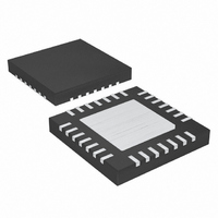
MAX8759ETI+ Maxim Integrated Products, MAX8759ETI+ Datasheet - Page 10

MAX8759ETI+
Manufacturer Part Number
MAX8759ETI+
Description
IC CNTRL CCFL BACKLIGHT 28TQFN
Manufacturer
Maxim Integrated Products
Type
CCFL Controllerr
Datasheet
1.MAX8759ETI.pdf
(32 pages)
Specifications of MAX8759ETI+
Frequency
30 ~ 80 kHz
Current - Supply
2.5mA
Voltage - Supply
4.5 V ~ 28 V
Operating Temperature
-40°C ~ 85°C
Package / Case
28-TQFN Exposed Pad
Lead Free Status / RoHS Status
Lead free / RoHS Compliant
Current - Output
-
Lead Free Status / Rohs Status
Details
Low-Cost, SMBus, CCFL Backlight Controller
10
PIN
10
11
12
13
14
15
16
17
______________________________________________________________________________________
1
2
3
4
5
6
7
8
9
PWMO
NAME
COMP
PWMI
FREQ
BATT
VALS
TFLT
ISEC
SDA
IFB1
IFB2
GH1
SCL
DEL
ALS
VFB
LX1
Supply Input. BATT is the input to the internal 5.35V linear regulator that powers the device. Bypass BATT
to GND with a 0.1µF ceramic capacitor.
SMBus Serial Data Input
SMBus Serial Clock Input
Fault-Timer Adjustment Pin. Connect a capacitor from TFLT to GND to set the time-out periods for open-
lamp and secondary overcurrent faults.
Ambient-Light-Sensor Supply Pin. Bypass VALS to GND with a 0.1µF capacitor.
Ambient-Light-Sensor Input
DPST Control Input
DPST Buffer Output. Connect a capacitor between PWMO and GND. The capacitor forms a lowpass filter
with an internal 40kΩ (typ) resistor for filtering the DPST signal.
Chopping-Frequency Adjustment Pin. Connect a resistor from FREQ to GND to set the DPWM frequency:
f
Transconductance Error Amplifier Output. A compensation capacitor connected between COMP and GND
sets the rise and fall time of the lamp-current envelope in DPWM operation.
Adaptive Zero-Crossing-Delay Adjustment Pin. Connect a resistor between DEL and GND to adjust the
range of the zero-crossing delay. Connecting DEL to V
Lamp-Current-Feedback Input. The IFB1 sense signal is internally full-wave rectified. IFB1 is compared
with IFB2 and the larger is used for lamp-current regulation. The average value of the rectified signal is
regulated to 785mV (typ) by controlling the on-time of high-side switch. An open-lamp fault is generated if
the peak voltage of IFB1 is below 600mV for a fault delay period set by TFLT.
Lamp-Current-Feedback Input. The IFB2 sense signal is internally full-wave rectified. IFB1 is compared
with IFB2 and the larger is used for lamp-current regulation. The average value of the rectified signal is
regulated to 800mV (typ) by controlling the on-time of high-side switch. An open-lamp fault is generated if
the peak voltage of IFB2 is below 600mV for a fault-delay period set by TFLT. IFB2 input can be disabled
by connecting IFB2 to V
Transformer Secondary Voltage-Feedback Input. A capacitive voltage-divider between the high-voltage
terminal of the CCFL tube and GND sets the maximum average lamp voltage during striking and lamp-out
fault. When the peak voltage on VFB exceeds the internal overvoltage threshold, the controller turns on an
internal current sink, discharging the COMP capacitor to limit the switch on-time. The VFB pin is also used
to detect a secondary undervoltage condition. If the peak voltage on VFB is below 230mV continuously for
250µs during the DPWM ON period, the MAX8759 shuts down.
Transformer Secondary Current-Feedback Input. A current-sense resistor connected between the low-
voltage end of the transformer secondary and the ground sets the maximum secondary current during
short-circuit fault. When the peak voltage on ISEC exceeds the internal overcurrent threshold, the
controller turns on an internal current sink discharging the COMP capacitor.
GH1 Gate-Driver Return. LX1 is the input to the current-limit and zero-crossing comparators. The device
senses the voltage across the low-side MOSFET NL1 to detect primary current zero crossing and primary
overcurrent.
High-Side MOSFET NH1 Gate Driver Output
DPWM
= 210Hz × 169kΩ / R
CC
.
FREQ
.
FUNCTION
CC
disables the zero-crossing delay function.
Pin Description


