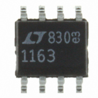
LTC1163CS8#PBF Linear Technology, LTC1163CS8#PBF Datasheet - Page 4

LTC1163CS8#PBF
Manufacturer Part Number
LTC1163CS8#PBF
Description
IC MOSFET DVR HI-SIDE TRPL 8SOIC
Manufacturer
Linear Technology
Datasheet
1.LTC1163CS8PBF.pdf
(8 pages)
Specifications of LTC1163CS8#PBF
Configuration
High-Side
Input Type
Non-Inverting
Delay Time
130µs
Number Of Configurations
3
Number Of Outputs
3
Voltage - Supply
1.8 V ~ 6 V
Operating Temperature
0°C ~ 70°C
Mounting Type
Surface Mount
Package / Case
8-SOIC (3.9mm Width)
Lead Free Status / RoHS Status
Lead free / RoHS Compliant
Current - Peak
-
High Side Voltage - Max (bootstrap)
-
Available stocks
Company
Part Number
Manufacturer
Quantity
Price
OPERATIO
PI FU CTIO S
LTC1163/LTC1165
TYPICAL PERFOR
Input Pins
The LTC1163 is noninverting; i.e., the MOSFET gate is
driven above the supply when the input pin is held high.
The LTC1165 is inverting and drives the MOSFET gate high
when the input pin is held low. The inverting inputs of the
LTC1165 allow P-channel switches to be replaced by
lower resistance/cost N-channel switches while maintain-
ing system drive polarity.
The LTC1163/LTC1165 logic inputs are high impedance
CMOS gates with ESD protection diodes to ground and
therefore should not be forced below ground. The inputs
can however, be driven above the power supply rail as
there are no clamping diodes connected between the input
pins and supply pin. This facilitates operation in mixed
5V/3V systems.
The LTC1163/LTC1165 are triple micropower MOSFET
drivers designed for operation over the 1.8V to 6V supply
range and include the following functional blocks:
3V Logic Compatible Inputs
The LTC1163/LTC1165 inputs have been designed to
accommodate a wide range of 3V and 5V logic families.
4
U
–1
5
4
3
2
1
0
Standby Supply Current
0
10
U
20
TEMPERATURE (°C)
30
U
U
40
50
LTC1163/65 • TPC07
W
60
A
U
70
CE
C
HARA TERISTICS
300
250
200
150
100
50
0
0
Supply Current per Driver ON
10
C
20
TEMPERATURE (°C)
30
V
V
Output Pins
The output pin is either driven to ground when the switch
is turned OFF or driven above the supply rail when the
switch is turned ON. The output is clamped to about 14V
above ground by a built-in Zener clamp. This pin has a
relatively high impedance when driven above the rail (the
equivalent of a few hundred k ). Care should be taken to
minimize any loading of this pin by parasitic resistance to
ground or supply.
Supply Pin
A 150
ground pin or supply pin if negative supply voltage tran-
sients are anticipated. This will limit the current flowing
from the power source into the LTC1163/LTC1165 to tens
of milliamps during reverse battery conditions.
The input threshold voltage is set at roughly 50% of the
supply voltage and approximately 200mV of input hyster-
esis is provided to ensure clean switching.
The input enables all of the following circuit blocks: the
bias generator, the high frequency oscillator and gate
charge pump. Therefore, when the input is turned off, the
entire circuit powers down and the supply current drops
below 1 A.
V
S
S
S
= 3.3V
= 1.8V
40
= 5V
50
LTC1163/65 • TPC08
resistor should be inserted in series with the
60
70
1000
100
0.1
10
1
0
MOSFET Gate Drive Current
T
A
= 25°C
GATE VOLTAGE ABOVE SUPPLY (V)
V
2
S
= 1.8V
4
V
S
V
= 3.3V
S
= 2.2V
6
LTC1163/65 • TPC09
V
S
8
= 5V
10


