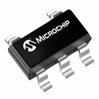
MCP1401T-E/OT Microchip Technology, MCP1401T-E/OT Datasheet - Page 3

MCP1401T-E/OT
Manufacturer Part Number
MCP1401T-E/OT
Description
IC MOSFET DRVR INV 500MA SOT23-5
Manufacturer
Microchip Technology
Type
Low Sider
Datasheet
1.MCP1401T-EOT.pdf
(20 pages)
Specifications of MCP1401T-E/OT
Number Of Outputs
1
Configuration
Low-Side
Input Type
Inverting
Delay Time
35ns
Current - Peak
500mA
Number Of Configurations
1
Voltage - Supply
4.5 V ~ 18 V
Operating Temperature
-40°C ~ 125°C
Mounting Type
Surface Mount
Package / Case
SOT-23-5, SC-74A, SOT-25
Rise Time
25 ns
Fall Time
20 ns
Supply Voltage (min)
4.5 V
Supply Current
1.1 mA
Maximum Power Dissipation
390 mW
Maximum Operating Temperature
+ 125 C
Mounting Style
SMD/SMT
Minimum Operating Temperature
- 40 C
Number Of Drivers
1
Lead Free Status / RoHS Status
Lead free / RoHS Compliant
High Side Voltage - Max (bootstrap)
-
Lead Free Status / Rohs Status
Lead free / RoHS Compliant
Other names
MCP1401T-E/OT
MCP1401T-E/OTTR
MCP1401T-E/OTTR
Available stocks
Company
Part Number
Manufacturer
Quantity
Price
Company:
Part Number:
MCP1401T-E/OT
Manufacturer:
Microchip Technology
Quantity:
40 936
Company:
Part Number:
MCP1401T-E/OT
Manufacturer:
MOLEX
Quantity:
5 200
1.0
Absolute Maximum Ratings †
Supply Voltage ................................................................+20V
Input Voltage ............................... (V
Input Current (V
Package Power Dissipation (T
DC CHARACTERISTICS (NOTE 2)
© 2007 Microchip Technology Inc.
Electrical Specifications: Unless otherwise indicated, T
Input
Logic ‘1’, High Input Voltage
Logic ‘0’, Low Input Voltage
Input Current
Input Voltage
Output
High Output Voltage
Low Output Voltage
Output Resistance, High
Output Resistance, Low
Peak Output Current
Latch-Up Protection With-
stand Reverse Current
Switching Time (Note 1)
Rise Time
Fall Time
Delay Time
Delay Time
Power Supply
Supply Voltage
Power Supply Current
Note 1:
SOT-23-5...................................................................0.39W
2:
ELECTRICAL
CHARACTERISTICS
Parameters
Switching times ensured by design.
Tested during characterization, not production tested.
IN
>V
DD
)................................................50 mA
A
= 50
DD
o
C)
+ 0.3V) to (GND – 5V)
Sym
V
R
I
V
R
V
V
V
I
REV
V
t
t
I
t
I
I
PK
t
D1
D2
OH
IN
OL
OH
DD
OL
R
S
S
IH
IN
F
IL
V
DD
Min
2.4
4.5
– 0.025
–1
—
—
—
—
—
—
—
—
—
—
—
—
-5
A
>0.5
0.85
0.10
Typ
1.5
1.3
0.5
= +25°C, with 4.5V ≤ V
12
10
19
15
35
35
—
—
—
—
—
† Notice: Stresses above those listed under "Maximum
Ratings" may cause permanent damage to the device. This is
a stress rating only and functional operation of the device at
those or any other conditions above those indicated in the
operational sections of this specification is not intended.
Exposure to maximum rating conditions for extended periods
may affect device reliability.
V
DD
0.025
Max
18.0
0.20
0.8
1.1
18
16
25
20
40
40
—
—
—
—
1
+0.3
Units
mA
mA
µA
ns
ns
ns
ns
Ω
Ω
V
V
V
V
V
A
A
V
DD
0V ≤ V
DC Test
DC Test
I
I
V
Duty cycle ≤ 2%, t ≤ 300 µs
Figure
C
Figure
C
Figure
Figure
V
V
OUT
OUT
MCP1401/02
≤ 18V.
DD
IN
IN
L
L
= 470 pF
= 470 pF
= 3V
= 0V
= 18V (Note 2)
= 10 mA, V
= 10 mA, V
IN
4-1,
4-1,
4-1,
4-1,
≤ V
Conditions
Figure 4-2
Figure 4-2
Figure 4-2
Figure 4-2
DD
DD
DD
DS22052B-page 3
= 18V
= 18V


