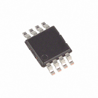
MAX5075AAUA+ Maxim Integrated Products, MAX5075AAUA+ Datasheet - Page 2

MAX5075AAUA+
Manufacturer Part Number
MAX5075AAUA+
Description
IC DRVR FET P-P 8-UMAX
Manufacturer
Maxim Integrated Products
Type
Low Sider
Datasheet
1.MAX5075AAUA.pdf
(8 pages)
Specifications of MAX5075AAUA+
Configuration
Low-Side
Input Type
Self Oscillating
Current - Peak
3A
Number Of Configurations
2
Number Of Outputs
2
Voltage - Supply
4.5 V ~ 15 V
Operating Temperature
-40°C ~ 125°C
Mounting Type
Surface Mount
Package / Case
8-MSOP, Micro8™, 8-uMAX, 8-uSOP,
Rise Time
10 ns
Fall Time
10 ns
Supply Voltage (min)
4.5 V
Supply Current
1 mA
Maximum Power Dissipation
825 mW
Maximum Operating Temperature
+ 125 C
Mounting Style
SMD/SMT
Minimum Operating Temperature
- 40 C
Number Of Drivers
2
Lead Free Status / RoHS Status
Lead free / RoHS Compliant
Delay Time
-
High Side Voltage - Max (bootstrap)
-
Lead Free Status / Rohs Status
Lead free / RoHS Compliant
ABSOLUTE MAXIMUM RATINGS
V
CLK, RT to DGND.....................................................-0.3V to +6V
NDRV1, NDRV2 to PGND...........................-0.3V to (V
DGND to PGND.....................................................-0.3V to +0.3V
CLK Current......................................................................±20mA
NDRV1, NDRV2 Peak Current (200ns) ..................................±5A
NDRV1, NDRV2 Reverse Current (Latchup Current)......±500mA
Push-Pull FET Driver with Integrated Oscillator
and Clock Output
Stresses beyond those listed under “Absolute Maximum Ratings” may cause permanent damage to the device. These are stress ratings only, and functional
operation of the device at these or any other conditions beyond those indicated in the operational sections of the specifications is not implied. Exposure to
absolute maximum rating conditions for extended periods may affect device reliability.
ELECTRICAL CHARACTERISTICS
(V
at T
Note 1: The MAX5075 is 100% tested at T
Note 2: Use the following formula to calculate the MAX5075 oscillator frequency: f
Note 3: The accuracy of the oscillator’s frequency is lower at frequencies greater than 1MHz.
2
SUPPLY
Input Voltage Supply Range
Switching Supply Current
Undervoltage Lockout
UVLO Hysteresis
OSCILLATOR
Frequency Range
Accuracy
Oscillator Jitter
CLK Output High Voltage
CLK Output Low Voltage
CLK Output Rise Time
CLK Output Fall Time
GATE DRIVERS (NDRV1, NDRV2)
Output High Voltage
Output Low Voltage
Output Peak Current
Driver Output Impedance
Latchup Current Protection
Rise Time
Fall Time
CC
CC
A
_______________________________________________________________________________________
to DGND, PGND .............................................-0.3V to +18V
= +12V, R
= +25°C.) (Note 1)
PARAMETER
RT
= 124kΩ, NDRV1 = NDRV2 = open, T
SYMBOL
I
V
CCSW
f
V
V
UVLO
V
OSC
I
t
t
CC
OH
OL
P
R
F
A
= T
J
= +125°C. All limits over temperature are guaranteed by design.
f
V
(Note 2)
f
I
I
C
C
I
I
Sourcing and sinking
NDRV_ sourcing 100mA
NDRV_ sinking 100mA
Reverse current at NDRV1/NDRV2
C
C
OSC
OSC
CLK
CLK
NDRV1
NDRV1
CC
CLK
CLK
LOAD
LOAD
CC
rising
= 1mA
= -1mA
A
= 250kHz
= 250kHz , 6V ≤ V
+ 0.3V)
= 30pF
= 30pF
= T
= 2nF
= 2nF
= I
= I
NDRV2
NDRV2
J
= -40°C to +125°C, unless otherwise noted. Typical values are measured
CONDITIONS
= 100mA
= -100mA
Continuous Power Dissipation (T
Operating Temperature Range .........................-40°C to +125°C
Maximum Junction Temperature .....................................+150°C
Storage Temperature Range .............................-60°C to +150°C
Lead Temperature (soldering, 10s) .................................+300°C
8-Pin µMAX (derate 10.3mW/°C above +70°C) ...........825mW
CC
7V ≤ V
4.5V ≤ V
≤ 15V (Note 3)
CC
CC
OSC
≤ 15V
≤ 7V
= 10
12
/(32 x R
V
3.35
MIN
4.5
3.9
0.3
CC
50
-8
3
RT
A
-
).
= +70°C)
±0.6
TYP
300
400
3.5
1.8
1.6
35
10
10
10
1
3
MAX
1500
15.0
+10
5.0
5.0
0.3
2.6
50
3
4
3
UNITS
kHz
mA
mV
mV
mA
ns
ns
ns
ns
%
%
Ω
V
V
V
V
V
A


