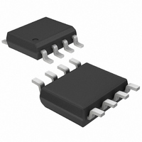
MAX15012AASA+ Maxim Integrated Products, MAX15012AASA+ Datasheet - Page 10

MAX15012AASA+
Manufacturer Part Number
MAX15012AASA+
Description
IC DRIVER MOSFET 8-SOIC
Manufacturer
Maxim Integrated Products
Type
High Side/Low Sider
Datasheet
1.MAX15013CASA.pdf
(18 pages)
Specifications of MAX15012AASA+
Configuration
Half Bridge
Input Type
Non-Inverting
Delay Time
30ns
Current - Peak
2A
Number Of Configurations
1
Number Of Outputs
2
High Side Voltage - Max (bootstrap)
175V
Voltage - Supply
8 V ~ 12.6 V
Operating Temperature
-40°C ~ 125°C
Mounting Type
Surface Mount
Package / Case
8-SOIC (3.9mm Width)
Rise Time
65 ns
Fall Time
65 ns
Supply Voltage (min)
8 V
Supply Current
3 mA
Maximum Power Dissipation
470.6 mW
Maximum Operating Temperature
+ 125 C
Mounting Style
SMD/SMT
Bridge Type
Half Bridge
Maximum Turn-off Delay Time
30 ns
Maximum Turn-on Delay Time
30 ns
Minimum Operating Temperature
- 40 C
Number Of Drivers
2
Lead Free Status / RoHS Status
Lead free / RoHS Compliant
The MAX15012/MAX15013 use a single-shot level-shifter
architecture to achieve low propagation delay. Typical
level shifter architecture causes a minimum (high or low)
pulse width (t
the logic-input pulse width. For the MAX15012/
MAX15013 devices, the DH minimum high pulse-width
(t
width (t
absence of external BBM delay during the narrow pulse
at low duty cycle. See Figure 2.
175V/2A, High-Speed,
Half-Bridge MOSFET Drivers
Figure 2. Minimum Pulse-Width Behavior for Narrow Duty-Cycle Input (On-Time < t
10
Dmin-DH-H
______________________________________________________________________________________
Dmin-DL-L
) is lower than the DL minimum low pulse
Dmin
) at the output that may be higher than
) to avoid any shoot-through in the
PW-MIN
Minimum Input Pulse Width
PW-MIN
DH
DL
V
DD
INH
INL
MAX15012D/
MAX15012B/
MAX15013B/
MAX15013D
t
DMIN-DH-H
t
DMIN-DL-L
At high duty cycle (close to 100%), the DH minimum low
pulse width (t
imum low pulse width (t
and shoot-through. See Figure 3. In case of the
MAX15012/MAX15013, there is a possibility of about
40ns overlap if an external BBM delay is not provided. It
is recommended to add external delay in the INH path
so that the minimum low pulse width seen at INH is
always longer than t
Characteristics table for the typical values of t
DH
HS
DL
PW-min
IN-BUILT
DEAD TIME
Dmin-DH-L
)
V
IN
N
N
) must be higher than the DL min-
Dmin-DL-L
PW-min
. See the Electrical
) to avoid the overlap
V
OUT
PW-min
.


