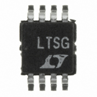
LTC1693-5CMS8 Linear Technology, LTC1693-5CMS8 Datasheet - Page 5

LTC1693-5CMS8
Manufacturer Part Number
LTC1693-5CMS8
Description
IC MOSFET DVR P-CH SINGLE 8-MSOP
Manufacturer
Linear Technology
Datasheet
1.LTC1693-5CMS8.pdf
(8 pages)
Specifications of LTC1693-5CMS8
Configuration
High-Side
Input Type
Inverting and Non-Inverting
Delay Time
38ns
Current - Peak
1.5A
Number Of Configurations
1
Number Of Outputs
1
Voltage - Supply
4.5 V ~ 13.2 V
Operating Temperature
0°C ~ 70°C
Mounting Type
Surface Mount
Package / Case
8-MSOP, Micro8™, 8-uMAX, 8-uSOP,
Lead Free Status / RoHS Status
Contains lead / RoHS non-compliant
High Side Voltage - Max (bootstrap)
-
Available stocks
Company
Part Number
Manufacturer
Quantity
Price
Company:
Part Number:
LTC1693-5CMS8
Manufacturer:
LT
Quantity:
10 000
Part Number:
LTC1693-5CMS8
Manufacturer:
LINEAR/凌特
Quantity:
20 000
Part Number:
LTC1693-5CMS8#PBF
Manufacturer:
LINEAR/凌特
Quantity:
20 000
PIN
IN (Pin 1): Driver Input. The input has V
thresholds with hysteresis to improve noise immunity.
NC (Pins 2, 5, 6): No Connect.
PHASE (Pin 3): Output Polarity Select. Connect this pin to
V
this pin for inverting operation. The typical PHASE pin
input current when pulled low is 20 A.
TI I G DIAGRA
CC
W
U
or leave it floating for noninverting operation. Ground
FUNCTIONS
U
U
U
W
OUTPUT OPERATION
OUTPUT OPERATION
NONINVERTING
INVERTING
CC
INPUT
independent
V
INPUT RISE/FALL TIME < 10ns
IH
90%
10%
t
t
PLH
PHL
t
t
r
f
GND (Pin 4): Driver Ground. Connect to a low impedance
ground. The V
to this pin.
OUT (Pin 7): Driver Output.
V
nal P-MOSFET should also connect directly to this pin.
This minimizes the AC current path and improves signal
integrity.
CC
(Pin 8): Power Supply Input. The source of the exter-
t
PHL
V
IL
t
f
CC
bypass capacitor should connect directly
90%
10%
1693-5 TD
t
PLH
t
r
LTC1693-5
5


