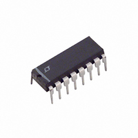
LT1158CN Linear Technology, LT1158CN Datasheet - Page 6

LT1158CN
Manufacturer Part Number
LT1158CN
Description
IC MOSFET DRVR 1/2BRDG NCH 16DIP
Manufacturer
Linear Technology
Datasheet
1.LT1158CNPBF.pdf
(22 pages)
Specifications of LT1158CN
Configuration
Half Bridge
Input Type
PWM
Current - Peak
500mA
Number Of Configurations
1
Number Of Outputs
2
High Side Voltage - Max (bootstrap)
56V
Voltage - Supply
5 V ~ 30 V
Operating Temperature
0°C ~ 70°C
Mounting Type
Through Hole
Package / Case
16-DIP (0.300", 7.62mm)
Lead Free Status / RoHS Status
Contains lead / RoHS non-compliant
Delay Time
-
Available stocks
Company
Part Number
Manufacturer
Quantity
Price
Part Number:
LT1158CN
Manufacturer:
LT/凌特
Quantity:
20 000
Part Number:
LT1158CN#PBF
Manufacturer:
LINEAR/凌特
Quantity:
20 000
PIN FUNCTIONS
LT1158
BOOST DR (Pin 1): Recharges and clamps the bootstrap
capacitor to 14.5V higher than pin 13 via an external
diode.
V
to the ground pin 7.
BIAS (Pin 3): Decouple point for the internal 2.6V bias
generator. Pin 3 cannot have any external DC loading.
ENABLE (Pin 4): When left open, the LT1158 operates
normally. Pulling pin 4 low holds both MOSFETs off re-
gardless of the input state.
FAULT (Pin 5): Open collector NPN output which turns
on when V12 – V11 exceeds the fault conduction thresh-
old.
INPUT (Pin 6): Taking pin 6 high turns the top MOSFET on
and bottom MOSFET off; pin 6 low reverses these states.
An input latch captures each low state, ignoring an ensuing
high until pin 13 has gone below 2.6V.
B GATE FB (Pin 8): Must connect directly to the bottom
power MOSFET gate. The top MOSFET turn-on is inhibited
until pin 8 has discharged to 1.5V. A hold-on current source
also feeds the bottom gate via pin 8.
B GATE DR (Pin 9): The high current drive point for the
bottom MOSFET. When a gate resistor is used, it is inserted
between pin 9 and the gate of the MOSFET.
6
+
(Pin 2): Main supply pin; must be closely decoupled
V
to the same supply as pin 2.
SENSE
limit comparator. Connects to the low side of a current
shunt or Kelvin lead of a current-sensing MOSFET. When
pin 11 is within 1.2V of V
SENSE
shunt or sense lead of a current-sensing MOSFET. A built-in
offset between pins 11 and 12 in conjunction with RSENSE
sets the top MOSFET short-circuit current.
T SOURCE (Pin 13): Top side driver return; connects to
MOSFET source and low side of the bootstrap capacitor.
T GATE FB (Pin 14): Must connect directly to the top power
MOSFET gate. The bottom MOSFET turn-on is inhibited
until V14 – V13 has discharged to 1.75V. An on-chip charge
pump also feeds the top gate via pin 14.
T GATE DR (Pin 15): The high current drive point for the
top MOSFET. When a gate resistor is used, it is inserted
between pin 15 and the gate of the MOSFET.
BOOST (Pin 16): Top side driver supply; connects to the
high side of the bootstrap capacitor and to a diode either
from supply (V
+
(Pin 10): Bottom side driver supply; must be connected
–
+
(Pin 12): Connects to the high side of the current
(Pin 11): The fl oating reference for the current
+
< 10V) or from pin 1 (V
+
, current limit is inhibited.
+
> 10V).
1158fb


