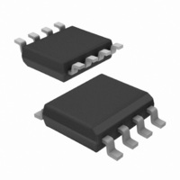
IR2128SPBF International Rectifier, IR2128SPBF Datasheet

IR2128SPBF
Specifications of IR2128SPBF
Related parts for IR2128SPBF
IR2128SPBF Summary of contents
Page 1
Floating channel designed for bootstrap operation Fully operational to +600V Tolerant to negative transient voltage dV/dt immune • Application- specific gate drive range: Motor Drive 20V (IR2127/IR2128) Automotive 20V (IR21271) • Undervoltage lockout • 3.3V, ...
Page 2
Absolute Maximum Ratings Absolute Maximum Ratings indicate sustained limits beyond which damage to the device may occur. All voltage param- eters are absolute voltages referenced to COM. The Thermal Resistance and Power Dissipation ratings are measured under board mounted and ...
Page 3
Dynamic Electrical Characteristics 15V 1000 pF and T BIAS are measured using the test circuit shown in Figure 3. Symbol Definition t Turn-On Propagation Delay on t Turn-Off Propagation ...
Page 4
Functional Block Diagram IR2127/IR21271 FAULT COM Functional Block Diagram IR2128 FAULT COM 4 UV DETECT R HV LEVEL R PULSE UP SHIFT FILTER SHIFTERS S PULSE V ...
Page 5
Lead Definitions Symbol Description V Logic and gate drive supply CC IN Logic input for gate driver output (HO), in phase with HO (IR2127/IR21271) Indicates over-current shutdown has occurred, negative logic FAULT COM Logic ground V High side floating supply ...
Page 6
IN (IR2128) IN (IR2127/ IR21271) CS FAULT HO Figure 1. Input/Output Timing Diagram V CSTH 90% Figure 4. CS Shutdown Waveform Definitions 6 IN 50% 50% (IR2128) 50% 50% IN (IR2127 ...
Page 7
Max. 200 100 Typ 0 -50 - Tem pe rature (°C) o Temperature ( C) Figure 10A Turn-On Time vs. Temperature 350 300 250 200 150 100 ...
Page 8
Max 100 . Typ 0 -50 - Temperature ( Tem perature (°C) C) Figure 12A Turn-On Rise Time vs. Temperature 200 150 100 Max. 50 Typ 0 . -50 -25 0 ...
Page 9
300 Typ. 200 100 0 -50 - Temperature ( C) Figure 15A CS Shutdown Propagation Delay vs. Temperature 800 700 600 500 Max. 400 Typ 300 200 100 0 -50 -25 ...
Page 10
Temperature ( C) Figure 18A Logic “0” Input Voltage (IR2127) Logic “1” Input Voltage (IR2128) vs Temperature 500 400 Max. 300 Typ. 200 100 Min. 0 -50 -25 ...
Page 11
Max. 0.2 0 -50 - Temperature ( C) Figure 21A Low Level Output vs Temperature 500 400 300 200 100 Max. 0 -50 - Temperature ( C) Figure ...
Page 12
Max . 150 Typ 100 . 50 0 -50 - Temperature ( C) Figure 24A Vcc Supply Current vs Temperature Max Typ 0 -50 -25 ...
Page 13
Max -50 - Temperature ( C) Figure 27A “High” CS Bias Current vs Temperature Max -50 - Temperature ( C) ...
Page 14
Max Typ. 9 Min -50 - Temperature (°C) o Temperature ( C) Figure 30A VBS Undervoltage Threshold (-) vs Temperature (IR2127/IR2128) 500 400 Typ. 300 200 Min. 100 ...
Page 15
Case outlines 0.25 [.010 0.25 [.010 NOT DIMENSIONING & TOLE RANCING PER AS ...
Page 16
... This product has been designed and qualified for the Industrial market. Qualification Standards can be found on IR’s Web site. Data and specifications subject to change without notice. Visit us at www.irf.com for sales contact information. order IR2127PbF order IR2127SPbF order IR21271PbF order IR2128PbF order IR2128SPbF TAC Fax: (310) 252-7903 09/08/04 www.irf.com ...


