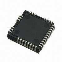
IR21363JPBF International Rectifier, IR21363JPBF Datasheet - Page 2

IR21363JPBF
Manufacturer Part Number
IR21363JPBF
Description
IC DRIVER 3-PHASE 44-PLCC
Manufacturer
International Rectifier
Specifications of IR21363JPBF
Configuration
3 Phase Bridge
Input Type
Inverting
Delay Time
425ns
Current - Peak
200mA
Number Of Configurations
1
Number Of Outputs
3
High Side Voltage - Max (bootstrap)
600V
Voltage - Supply
12 V ~ 20 V
Operating Temperature
-40°C ~ 125°C
Mounting Type
Surface Mount
Package / Case
44-PLCC (32 Leads)
Peak Output Current
350mA
Input Delay
525ns
Output Delay
500ns
Supply Voltage Range
12V To 20V
Driver Case Style
LCC
No. Of Pins
32
Operating Temperature Range
-40°C To +125°C
Rohs Compliant
Yes
Family Hvic
General Purpose HVICs
Channels
6
Topology
Three Phase
Application
General Purpose / Motor Control / PDP
Voffset
600
Io+ (ma)
200
Io- (ma)
350
Shutdown / Reset
Yes
Separate Power And Logic Ground
Yes
Over Current Protection
Yes
Uvlo
Vcc / Vbs
Vbsuv+ / Vccuv+ Min (v)
10.6
Vbsuv+ / Vccuv+ Typ (v)
11.1
Vbsuv+ / Vccuv+ Max (v)
11.6
Vbsuv- / Vccuv- Min (v)
10.4
Vbsuv- / Vccuv- Typ (v)
10.9
Dt / Sdt Min (ns)
220
Dt / Sdt Typ (ns)
290
Dt / Sdt Max (ns)
360
T On Min (ns)
300
T On Typ (ns)
425
T On Max (ns)
550
T Off Min (ns)
250
T Off Typ (ns)
400
T Off Max (ns)
550
Fault Reporting
Yes
Inverter Input Logic
LIN / HIN
Package
28 or 44 Lead
Part Status
Active & Preferred
Lead Free Status / RoHS Status
Lead free / RoHS Compliant
Available stocks
Company
Part Number
Manufacturer
Quantity
Price
Company:
Part Number:
IR21363JPBF
Manufacturer:
International Rectifier
Quantity:
10 000
IR21363 ( J&S)PbF
www.irf.com
Recommended Operating Conditions
The Input/Output logic timing diagram is shown in figure 1. For proper operation the device should be used within the recom-
mended conditions. All voltage parameters are absolute referenced to COM. The V S offset rating is tested with all supplies
biased at 15V differential.
Absolute Maximum Ratings
Absolute maximum ratings indicate sustained limits beyond which damage to the device may occur. All voltage parameters
are absolute voltages referenced to COM. The thermal resistance and power dissipation ratings are measured under board
mounted and still air conditions.
Note 1: Logic operational for V
Note 2: All input pins and the ITRIP pin are internally clamped with a 5.2V zener diode.
Symbol
Symbol
V
V
V
V
V
V
V
Rth
HO1,2,3
LO1,2,3
dV/dt
LO1,2,3
V
V
V
V
V
V
V
V
B1,2,3
S1,2,3
V
ITRIP
V
RCIN
V
P
T
T
T
T
FLT
FLT
CC
HO
CC
SS
BS
SS
IN
IN
A
S
D
S
L
J
JA
(Please refer to the Design Tip DT97-3 for more details).
High side floating supply voltage
High side floating supply offset voltage
High side output voltage
Low side output voltage
Low side and logic fixed supply voltage
Logic ground
FAULT output voltage
RCIN input voltage
ITRIP input voltage
Logic input voltage LIN , HIN
Ambient temperature
High side offset voltage
High side floating supply voltage
High side floating output voltage
Low side and logic fixed supply voltage
Logic ground
Low side output voltage
Input voltage LIN,HIN,ITRIP, EN, RCIN
FAULT output voltage
Allowable offset voltage slew rate
Package power dissipation @ T
Thermal resistance, junction to ambient
Junction temperature
Storage temperature
Lead temperature (soldering, 10 seconds)
S
of COM -5V to COM +600V. Logic state held for V
Definition
Definition
A
+25°C
(44
(44 lead PLCC)
lead
(28 lead PDIP)
(28 lead SOIC)
(28 lead SOIC)
(28 lead PDIP)
PLCC)
V
V
V
S1,2,3
V
V
V
S
B1,2,3
S1,2,3 +
Note 1
V
CC
SS
SS
Min.
Min.
of COM -5V to COM -V
V
V
V
S1,2,3
V
-0.3
-0.3
-0.3
-40
-55
12
—
—
—
—
—
—
—
—
—
-5
0
SS
SS
SS
SS
- 0.3
- 0.3
- 25
- 0.3
- 25
12
(V
V
V
V
V
V
B1,2,3
B1,2,3
V
V
SS
S1,2,3 +
V
V
lower of
CC
CC
V
CC
CC
Max.
Max.
SS
SS
V
V
V
600
B1,2,3
125
625
150
150
300
1.5
1.6
2.0
20
25
50
83
78
63
+ 15) or
CC
5
CC
CC
+ 0.3)
+ 0.3
+ 0.3
+ 0.3
+5
+5
+ 0.3
+ 0.3
20
BS
.
°C/W
Units
Units
V/ns
o
°C
C
W
V
V
2


