LM5101ASDX/NOPB National Semiconductor, LM5101ASDX/NOPB Datasheet - Page 6
LM5101ASDX/NOPB
Manufacturer Part Number
LM5101ASDX/NOPB
Description
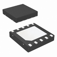
IC DVR HALF-BRIDGE HV 10-LLP
Manufacturer
National Semiconductor
Datasheet
1.LM5101CSDNOPB.pdf
(18 pages)
Specifications of LM5101ASDX/NOPB
Configuration
High and Low Side, Synchronous
Input Type
Non-Inverting
Delay Time
26ns
Current - Peak
3A
Number Of Configurations
1
Number Of Outputs
2
High Side Voltage - Max (bootstrap)
118V
Voltage - Supply
9 V ~ 14 V
Mounting Type
Surface Mount
Package / Case
10-LLP
Lead Free Status / RoHS Status
Lead free / RoHS Compliant
Operating Temperature
-
Other names
LM5101ASDX
Available stocks
Company
Part Number
Manufacturer
Quantity
Price
Company:

Part Number:
LM5101ASDX/NOPB
Manufacturer:
NS
Quantity:
18 000


www.national.com
I
THERMAL RESISTANCE
θ
t
t
t
t
t
t
t
t
t
Symbol
OLL
LPHL
LPLH
HPHL
HPLH
MON
MOFF
RC
R
F
JA
Symbol
Switching Characteristics
Limits in standard type are for T
+125°C. Minimum and Maximum limits are guaranteed through test, design, or statistical correlation. Typical values represent the
most likely parametric norm at T
12V, V
, t
FC
SS
Peak Pulldown Current LM5100A/LM5101A
Peak Pulldown Current LM5100B/LM5101B
Peak Pulldown Current LM5100C/LM5101C
Junction to Ambient
= V
LO Turn-Off Propagation Delay
LM5100A/B/C
LO Turn-Off Propagation Delay
LM5101A/B/C
LO Turn-On Propagation Delay
LM5100A/B/C
LO Turn-On Propagation Delay
LM5101A/B/C
HO Turn-Off Propagation Delay
LM5100A/B/C
HO Turn-Off Propagation Delay
LM5101A/B/C
LO Turn-On Propagation Delay
LM5100A/B/C
LO Turn-On Propagation Delay
LM5101A/B/C
Delay Matching: LO on & HO off
LM5100A/B/C
Delay Matching: LO on & HO off
LM5101A/B/C
Delay Matching: LO off & HO on
LM5100A/B/C
Delay Matching: LO on & HO off
LM5101A/B/C
Either Output Rise/Fall Time
Output Rise Time (3V to 9V) LM5100A/
LM5101A
Output Rise Time (3V to 9V) LM5100B/
LM5101B
Output Rise Time (3V to 9V) LM5100C/
LM5101C
Output Fall Time (3V to 9V) LM5100A/
LM5101A
Output Fall Time (3V to 9V) LM5100B/
LM5101B
Output Fall Time (3V to 9V) LM5100C/
LM5101C
HS
= 0V, No Load on LO or HO
Parameter
Parameter
J
J
= 25°C only; limits in boldface type apply over the junction temperature (T
= 25°C, and are provided for reference purposes only. Unless otherwise specified, V
(Note
4).
LI Falling to LO Falling
LI Rising to LO Rising
HI Falling to HO Falling
HI Rising to HO Rising
C
C
C
L
L
L
= 1000 pF
= 0.1 µF
= 0.1 µF
HO, LO = 12V
SOIC-8
LLP-8(Note
LLP-10
PSOP-8
eMSOP-8
Conditions
6
(Note
Conditions
(Note
3)
3)
3)
Min
Min
Typ
430
570
990
260
430
715
20
22
20
26
20
22
20
26
1
4
1
4
8
Typ
170
40
40
40
80
3
2
1
J
) range of -40°C to
Max
45
56
45
56
45
56
45
56
10
10
10
10
Max
DD
= V
Units
Units
°C/W
ns
ns
ns
ns
ns
ns
ns
ns
ns
HB
A
=
Related parts for LM5101ASDX/NOPB
Image
Part Number
Description
Manufacturer
Datasheet
Request
R

Part Number:
Description:
Manufacturer:
National Semiconductor
Datasheet:

Part Number:
Description:
IC DVR HALF-BRIDGE HV 10-LLP
Manufacturer:
National Semiconductor
Datasheet:
Part Number:
Description:
IC DVR HALF-BRIDGE HV 8-LLP
Manufacturer:
National Semiconductor
Datasheet:
Part Number:
Description:
IC,Dual MOSFET Driver,LLCC,10PIN,PLASTIC
Manufacturer:
National Semiconductor

Part Number:
Description:
High Voltage High Side and Low Side Gate Driver
Manufacturer:
NSC [National Semiconductor]
Datasheet:
Part Number:
Description:
National Semiconductor [8-Bit D/A Converter]
Manufacturer:
National Semiconductor
Datasheet:
Part Number:
Description:
National Semiconductor [Media Coprocessor]
Manufacturer:
National Semiconductor
Datasheet:
Part Number:
Description:
Digitally Controlled Tone and Volume Circuit with Stereo Audio Power Amplifier, Microphone Preamp Stage and National 3D Sound
Manufacturer:
National Semiconductor
Datasheet:
Part Number:
Description:
Digitally Controlled Tone and Volume Circuit with Stereo Audio Power Amplifier, Microphone Preamp Stage and National 3D Sound
Manufacturer:
National Semiconductor
Datasheet:
Part Number:
Description:
AC97 Rev 2 Codec with Sample Rate Conversion and National 3D Sound
Manufacturer:
National Semiconductor
Part Number:
Description:
Manufacturer:
National Semiconductor
Datasheet:
Part Number:
Description:
Manufacturer:
National Semiconductor
Datasheet:
Part Number:
Description:
General Purpose, Low Voltage, Low Power, Rail-to-Rail Output Operational Amplifiers
Manufacturer:
National Semiconductor
Datasheet:
Part Number:
Description:
8-bit 20 MSPS flash A/D converter.
Manufacturer:
National Semiconductor
Datasheet: