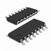
SI8232BB-B-IS1 Silicon Laboratories Inc, SI8232BB-B-IS1 Datasheet - Page 13

SI8232BB-B-IS1
Manufacturer Part Number
SI8232BB-B-IS1
Description
IC DUAL LOW SIDE DRIVER 16SOIC
Manufacturer
Silicon Laboratories Inc
Datasheets
1.SI8234BB-C-IS1.pdf
(52 pages)
2.SI8234BB-C-IS1.pdf
(8 pages)
3.SI8232BB-B-IS1.pdf
(52 pages)
Specifications of SI8232BB-B-IS1
Package / Case
16-SOIC (3.9mm Width)
Configuration
Low-Side
Input Type
Non-Inverting
Delay Time
60ns
Current - Peak
500mA
Number Of Configurations
2
Number Of Outputs
2
Voltage - Supply
6.5 V ~ 24 V
Operating Temperature
-40°C ~ 125°C
Mounting Type
Surface Mount
Mounting Style
SMD/SMT
Number Of Channels
2
Propagation Delay Time
30 ns
Supply Voltage (max)
5.5 V
Supply Voltage (min)
4.5 V
Supply Current
2 mA
Power Dissipation
1.2 W
Maximum Operating Temperature
+ 125 C
Minimum Operating Temperature
- 40 C
Number Of Drivers
2
Driver Configuration
Non-Inverting
Input Logic Level
TTL
Rise Time
20ns
Fall Time
20ns
Frequency (max)
8MHz
Operating Supply Voltage (max)
5.5/24V
Peak Output Current
500mA
Output Resistance
15Ohm
Operating Supply Voltage (min)
4.5/6.5V
Operating Temp Range
-40C to 125C
Operating Temperature Classification
Automotive
Mounting
Surface Mount
Pin Count
16
Package Type
SOIC N
Lead Free Status / RoHS Status
Lead free / RoHS Compliant
High Side Voltage - Max (bootstrap)
-
Lead Free Status / Rohs Status
Lead free / RoHS Compliant
Other names
336-1909-5
Available stocks
Company
Part Number
Manufacturer
Quantity
Price
Part Number:
SI8232BB-B-IS1
Manufacturer:
SILICON LABS/芯科
Quantity:
20 000
Table 6. IEC 60747-5-2 Insulation Characteristics*
Table 7. IEC Safety Limiting Values
Maximum Working Insulation
Voltage
Input to Output Test Voltage
Highest Allowable Overvolt-
age (Transient Overvoltage,
t
Pollution Degree (DIN VDE
0110, Table 1)
Insulation Resistance at T
V
*Note: The Si823x is suitable for basic electrical isolation within the safety limit data. Maintenance of the safety data is
Parameter
Case Temperature
Safety Input Current
Device Power
Dissipation
Notes:
TR
IO
1. Maximum value allowed in the event of a failure. Refer to the thermal derating curve in Figures 6 and 7.
2. The Si82xx is tested with V
= 60 sec)
= 500 V
ensured by protective circuits. The Si823x provides a climate classification of 40/125/21.
square wave.
Parameter
2
Symbol
P
T
I
S
S
D
S
,
105 °C/W (NB SOIC-16, 14 LD LGA),
DDI
Symbol
50 °C/W (14 LD LGA w/ Pad)
JA
V
V
V
= 5.5 V, V
IORM
R
T
= 100 °C/W (WB SOIC-16),
PR
TR
J
S
V
= 150 °C, T
DDA
Test Condition
V
1
DDI
= V
(V
Partial Discharge <
DDA
Production Test,
Test Condition
= 5.5 V,
IORM
DDB
t
Method b1
PR
m
= V
A
= 24 V,
5 pC)
= 1 sec,
= 25 °C
, 100%
x 1.875 = V
DDB
Rev. 1.0
= 24 V, T
J
= 150 ºC, C
SOIC-16
SOIC-16
WB
150
1.2
1375
6000
>10
50
WB
891
2
9
L
SOIC-16
= 100 pF, input 2 MHz 50% duty cycle
Characteristic
150
NB SOIC-16
NB
1.2
50
14 LD LGA
1050
4000
>10
560
2
9
LD LGA
150
1.2
50
14
14 LD LGA
w/ Pad
2650
>10
373
700
LGA w/
14 LD
2
Pad
150
100
1.2
Si823x
9
V peak
V peak
V peak
Unit
Unit
mA
°C
W
13


