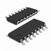
SI8232BB-B-IS1 Silicon Laboratories Inc, SI8232BB-B-IS1 Datasheet - Page 33

SI8232BB-B-IS1
Manufacturer Part Number
SI8232BB-B-IS1
Description
IC DUAL LOW SIDE DRIVER 16SOIC
Manufacturer
Silicon Laboratories Inc
Datasheets
1.SI8234BB-C-IS1.pdf
(52 pages)
2.SI8234BB-C-IS1.pdf
(8 pages)
3.SI8232BB-B-IS1.pdf
(52 pages)
Specifications of SI8232BB-B-IS1
Package / Case
16-SOIC (3.9mm Width)
Configuration
Low-Side
Input Type
Non-Inverting
Delay Time
60ns
Current - Peak
500mA
Number Of Configurations
2
Number Of Outputs
2
Voltage - Supply
6.5 V ~ 24 V
Operating Temperature
-40°C ~ 125°C
Mounting Type
Surface Mount
Mounting Style
SMD/SMT
Number Of Channels
2
Propagation Delay Time
30 ns
Supply Voltage (max)
5.5 V
Supply Voltage (min)
4.5 V
Supply Current
2 mA
Power Dissipation
1.2 W
Maximum Operating Temperature
+ 125 C
Minimum Operating Temperature
- 40 C
Number Of Drivers
2
Driver Configuration
Non-Inverting
Input Logic Level
TTL
Rise Time
20ns
Fall Time
20ns
Frequency (max)
8MHz
Operating Supply Voltage (max)
5.5/24V
Peak Output Current
500mA
Output Resistance
15Ohm
Operating Supply Voltage (min)
4.5/6.5V
Operating Temp Range
-40C to 125C
Operating Temperature Classification
Automotive
Mounting
Surface Mount
Pin Count
16
Package Type
SOIC N
Lead Free Status / RoHS Status
Lead free / RoHS Compliant
High Side Voltage - Max (bootstrap)
-
Lead Free Status / Rohs Status
Lead free / RoHS Compliant
Other names
336-1909-5
Available stocks
Company
Part Number
Manufacturer
Quantity
Price
Part Number:
SI8232BB-B-IS1
Manufacturer:
SILICON LABS/芯科
Quantity:
20 000
DISABLE
GNDB
VDDB
GNDA
VDDA
GNDI
VDDI
VDDI
VOB
VOA
Pin
VIA
VIB
NC
DT
Name
10
11
12
13
14
1
2
3
4
5
6
7
8
9
Table 14. Si8233 Two-Input HS/LS Isolated Driver (14 LD LGA)
Input-side ground terminal.
Non-inverting logic input terminal for Driver A.
Non-inverting logic input terminal for Driver B.
Input-side power supply terminal; connect to a source of 4.5 to 5.5 V.
Device Disable. When high, this input unconditionally drives outputs VOA, VOB LOW.
It is strongly recommended that this input be connected to external logic level to avoid
erroneous operation due to capacitive noise coupling.
Dead time programming input. The value of the resistor connected from DT to ground
sets the dead time between output transitions of VOA and VOB. Defaults to 1 ns dead
time when connected to VDDI or left open (see"3.8.Programmable Dead Time and
Overlap Protection" on page 26).
Input-side power supply terminal; connect to a source of 4.5 to 5.5 V.
Ground terminal for Driver B.
Driver B output (low-side driver).
Driver B power supply voltage terminal; connect to a source of 6.5 to 24 V.
No connection.
Ground terminal for Driver A.
Driver A output (high-side driver).
Driver A power supply voltage terminal; connect to a source of 6.5 to 24 V.
DISABLE
GNDI
VDDI
VDDI
VIA
VIB
DT
1
2
3
4
5
6
7
LGA-14 (5 x 5 mm)
Rev. 1.1
Si8233
Description
14
13
12
11
10
7
8
GNDB
VDDA
VOA
GNDA
NC
VDDB
VOB
Si823x
33


