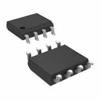
LM5110-3M/NOPB National Semiconductor, LM5110-3M/NOPB Datasheet - Page 10

LM5110-3M/NOPB
Manufacturer Part Number
LM5110-3M/NOPB
Description
IC DRIVER DUAL 5A NEG VOUT 8SOIC
Manufacturer
National Semiconductor
Datasheet
1.LM5110-1MNOPB.pdf
(13 pages)
Specifications of LM5110-3M/NOPB
Configuration
Low-Side
Input Type
Inverting and Non-Inverting
Delay Time
25ns
Current - Peak
5A
Number Of Configurations
2
Number Of Outputs
2
Voltage - Supply
3.5 V ~ 14 V
Operating Temperature
-40°C ~ 125°C
Mounting Type
Surface Mount
Package / Case
8-SOIC (3.9mm Width)
Lead Free Status / RoHS Status
Lead free / RoHS Compliant
High Side Voltage - Max (bootstrap)
-
Other names
*LM5110-3M
*LM5110-3M/NOPB
LM5110-3M
*LM5110-3M/NOPB
LM5110-3M
www.national.com
Thermal Performance
The schematic above shows a conceptual diagram of the
LM5110 output and MOSFET load. Q1 and Q2 are the
switches within the gate driver. R
the external MOSFET, and C
tance of the MOSFET. The gate resistance Rg is usually very
small and losses in it can be neglected. The equivalent gate
capacitance is a difficult parameter to measure since it is the
combination of C
(gate to drain capacitance). Both of these MOSFET capaci-
tances are not constants and vary with the gate and drain
voltage. The better way of quantifying gate capacitance is
the total gate charge Q
charge required by C
voltage V
Assuming negligible gate resistance, the total power dissi-
pated in the MOSFET driver due to gate charge is approxi-
mated by
Where
F
As an example, consider the MOSFET MTD6N15 whose
gate charge specified as 30 nC for V
The power dissipation in the driver due to charging and
discharging of MOSFET gate capacitances at switching fre-
quency of 300 kHz and V
If both channels of the LM5110 are operating at equal fre-
quency with equivalent loads, the total losses will be twice as
this value which is 0.216W.
In addition to the above gate charge power dissipation, -
transient power is dissipated in the driver during output
transitions. When either output of the LM5110 changes state,
current will flow from V
time through the output totem-pole N and P channel
MOSFETs. The final component of power dissipation in the
driver is the power associated with the quiescent bias cur-
rent consumed by the driver input stage and Under-voltage
lockout sections.
Characterization of the LM5110 provides accurate estimates
of the transient and quiescent power dissipation compo-
nents. At 300 kHz switching frequency and 30 nC load used
SW
= switching frequency of the MOSFET.
P
DRIVER
GATE
.
P
= 12V x 30 nC x 300 kHz = 0.108W.
DRIVER
GS
(gate to source capacitance) and C
GS
CC
= V
G
GATE
and C
to V
in coloumbs. Q
GATE
IN
is the equivalent gate capaci-
EE
of 12V is equal to
GD
x Q
G
for a very brief interval of
is the gate resistance of
G
for a given gate drive
GATE
x F
(Continued)
SW
= 12V.
G
combines the
GD
FIGURE 2.
10
in the example, the transient power will be 8 mW. The 1 mA
nominal quiescent current and 12V V
12 mW typical quiescent power.
Therefore the total power dissipation
We know that the junction temperature is given by
Or the rise in temperature is given by
For SOIC-8 package θ
conditions of natural convection.
Therefore T
For LLP-10 package, the integrated circuit die is attached to
leadframe die pad which is soldered directly to the printed
circuit board. This substantially decreases the junction to
ambient thermal resistance (θ
achievable with the LLP10 package. The resulting T
the dual driver example above is thereby reduced to just 9.5
degrees.
CONTINUOUS CURRENT RATING OF LM5110
The LM5110 can deliver pulsed source/sink currents of 3A
and 5A to capacitive loads. In applications requiring continu-
ous load current (resistive or inductive loads), package
power dissipation, limits the LM5110 current capability far
below the 5A sink/3A source capability. Rated continuous
current can be estimated both when sourcing current to or
sinking current from the load. For example when sinking, the
maximum sink current can be calculated as
where R
output stage of LM5110.
Consider T
package under the condition of natural convection and no air
flow. If the ambient temperature (T
DS
P
(on) is the on resistance of lower MOSFET in the
J
D
RISE
(max) of 125˚C and θ
= 0.216 + 0.008 + 0.012 = 0.236W.
T
20079207
T
RISE
is equal to
RISE
T
= 0.236 x 170 = 40.1˚C
J
= T
= P
JA
J
is estimated as 170˚C/W for the
D
− T
x θ
JA
A
JA
). θ
= P
JA
+ T
A
JA
of 170˚C/W for an SO-8
D
) is 60˚C, and the R
GATE
A
x θ
as low as 40˚C/W is
JA
supply produce a
RISE
for
D -


