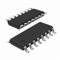
SI8233BB-C-IS1 Silicon Laboratories Inc, SI8233BB-C-IS1 Datasheet - Page 6

SI8233BB-C-IS1
Manufacturer Part Number
SI8233BB-C-IS1
Description
IC HIGH/LOW SIDE DRIVER 16SOIC
Manufacturer
Silicon Laboratories Inc
Specifications of SI8233BB-C-IS1
Package / Case
16-SOIC (3.9mm Width)
Configuration
High or Low Side
Input Type
Non-Inverting
Delay Time
60ns
Current - Peak
4A
Number Of Configurations
2
Number Of Outputs
2
Voltage - Supply
6.5 V ~ 24 V
Operating Temperature
-40°C ~ 125°C
Mounting Type
Surface Mount
Mounting Style
SMD/SMT
Number Of Channels
2
Propagation Delay Time
30 ns
Supply Voltage (max)
5.5 V
Supply Voltage (min)
4.5 V
Supply Current
2 mA
Power Dissipation
1.2 W
Maximum Operating Temperature
+ 125 C
Minimum Operating Temperature
- 40 C
Number Of Drivers
2
Driver Configuration
Non-Inverting
Driver Type
High and Low Side
Input Logic Level
TTL
Rise Time
12ns
Fall Time
12ns
Frequency (max)
8MHz
Operating Supply Voltage (max)
5.5/24V
Peak Output Current
4A
Output Resistance
2.7Ohm
Operating Supply Voltage (min)
4.5/6.5V
Operating Temp Range
-40C to 125C
Operating Temperature Classification
Automotive
Mounting
Surface Mount
Pin Count
16
Package Type
SOIC N
Lead Free Status / RoHS Status
Lead free / RoHS Compliant
High Side Voltage - Max (bootstrap)
-
Lead Free Status / Rohs Status
Lead free / RoHS Compliant
Other names
336-1905-5
339-1905-5
339-1905-5
339-1905-5
339-1905-5
Si823x
2. Electrical Specifications
Table 1. Electrical Characteristics
4.5 V < VDDI < 5.5 V, VDDA = VDDB = 12 V or 15 V. TA = –40 to +125 °C. Typical specs at 25 °C
6
Parameter
DC Specifications
Input-side Power Supply
Voltage
Driver Supply Voltage
Input Supply Quiescent
Current
Output Supply Quiescent
Current
Input Supply Active Current
Output Supply Active Current
Input Pin Leakage Current
Input Pin Leakage Current
Logic High Input Threshold
Logic Low Input Threshold
Input Hysteresis
Logic High Output Voltage
Logic Low Output Voltage
Output Short-Circuit Pulsed
Sink Current
Output Short-Circuit Pulsed
Source Current
Output Sink Resistance
Output Source Resistance
Notes:
1. VDDA = VDDB = 12 V for 5, 8, and 10 V UVLO devices; VDDA = VDDB = 15 V for 12.5 V UVLO devices.
2. TDD is the minimum overlap time without triggering overlap protection (Si8230/1/3/4 only).
3. The largest RDT resistor that can be used is 220 k.
VDDA, VDDB
VOAL, VOBL
R
IOA(SCH),
IVIA, IVIB,
IDISABLE
IOA(SCL),
IOB(SCH)
ON(SOURCE)
IOB(SCL)
R
IDDA(Q),
IDDB(Q)
Symbol
IDDI(Q)
VOAH,
VI
VOBH
ON(SINK)
IPWM
IDDO
VDDI
IDDI
VIH
VIL
HYST
1
GNDA, and VDDB and GNDB
Voltage between VDDA and
(See “6. Ordering Guide” )
Si8233/4/5/6, Figure 4
Si8233/4/5/6, Figure 5
PWM freq = 500 kHz
PWM freq = 500 kHz
Si8230/1/2, Figure 4
Si8230/1/2, Figure 5
Current per channel
Si8230/32/33/35/36
Rev. 1.1
IOA, IOB = –1 mA
Test Conditions
IOA, IOB = 1 mA
Si8233/4/5/6
Si8233/4/5/6
Si8230/1/2
Si8230/1/2
Si8231/34
/VDDB)
— 0.04
(VDDA
Min
–10
–10
400
4.5
6.5
2.0
—
—
—
—
—
—
—
—
—
—
—
—
—
—
—
0.25
Typ
450
2.5
3.6
0.5
4.0
2.0
5.0
1.0
2.7
—
—
—
—
—
—
15
—
—
—
2
2
Max
0.04
+10
+10
5.5
3.0
0.8
24
—
—
—
—
—
—
—
—
—
—
—
—
—
3
3
Units
µA dc
µA dc
mA
mA
mA
mA
mA
mV
V
V
V
V
V
V
A


