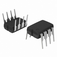
MC33153PG ON Semiconductor, MC33153PG Datasheet - Page 2

MC33153PG
Manufacturer Part Number
MC33153PG
Description
IC DRIVER GATE SINGLE IGBT 8DIP
Manufacturer
ON Semiconductor
Type
Single IGBT Gate Driverr
Datasheet
1.MC33153PG.pdf
(13 pages)
Specifications of MC33153PG
Configuration
Low-Side
Input Type
Non-Inverting
Delay Time
80ns
Current - Peak
1A
Number Of Configurations
1
Number Of Outputs
1
Voltage - Supply
11 V ~ 20 V
Operating Temperature
-40°C ~ 105°C
Mounting Type
Through Hole
Package / Case
8-DIP (0.300", 7.62mm)
Supply Current
20 mA
Mounting Style
Through Hole
Lead Free Status / RoHS Status
Lead free / RoHS Compliant
High Side Voltage - Max (bootstrap)
-
Lead Free Status / Rohs Status
Lead free / RoHS Compliant
Other names
MC33153PGOS
Available stocks
Company
Part Number
Manufacturer
Quantity
Price
Company:
Part Number:
MC33153PG
Manufacturer:
IXSY
Quantity:
772
Company:
Part Number:
MC33153PG
Manufacturer:
ON Semiconductor
Quantity:
422
Part Number:
MC33153PG
Manufacturer:
ON/安森美
Quantity:
20 000
NOTE:
Stresses exceeding Maximum Ratings may damage the device. Maximum Ratings are stress ratings only. Functional operation above the
Recommended Operating Conditions is not implied. Extended exposure to stresses above the Recommended Operating Conditions may affect
device reliability.
1. Kelvin Ground must always be between V
2. Low duty cycle pulse techniques are used during test to maintain the junction temperature as close to ambient as possible.
MAXIMUM RATINGS
ELECTRICAL CHARACTERISTICS
for min/max values T
LOGIC INPUT
DRIVE OUTPUT
FAULT OUTPUT
SWITCHING CHARACTERISTICS
Power Supply Voltage
Logic Input
Current Sense Input
Blanking/Desaturation Input
Gate Drive Output
Fault Output
Power Dissipation and Thermal Characteristics
Operating Junction Temperature
Operating Ambient Temperature
Storage Temperature Range
Input Threshold Voltage
Input Current
Output Voltage
Output Pull−Down Resistor
Output Voltage
Propagation Delay (50% Input to 50% Output C
Drive Output Rise Time (10% to 90%) C
Drive Output Fall Time (90% to 10%) C
Propagation Delay
T
Source Current
Sink Current
Diode Clamp Current
Source Current
Sink Current
D Suffix SO−8 Package, Case 751
P Suffix DIP−8 Package, Case 626
High State (Logic 1)
Low State (Logic 0)
High State (V
Low State (V
Low State (I
High State (I
Low State (I
High State (I
Logic Input to Drive Output Rise
Logic Input to Drive Output Fall
low
= −40°C for MC33153
Maximum Power Dissipation @ T
Thermal Resistance, Junction−to−Air
Maximum Power Dissipation @ T
Thermal Resistance, Junction−to−Air
ESD data available upon request.
Sink
Sink
Source
Source
IL
IH
= 1.2 V)
= 3.0 V)
= 1.0 A)
= 5.0 mA)
A
is the operating ambient temperature range that applies (Note 2), unless otherwise noted.)
= 500 mA)
= 20 mA)
Current Sense Input to Drive Output
Fault Blanking/Desaturation Input to Drive Output
V
Kelvin Ground to V
CC
Characteristic
to V
T
high
Rating
EE
= +105°C for MC33153
L
L
A
A
= 1.0 nF
(V
= 1.0 nF
= 50°C
= 50°C
EE
CC
EE
and V
= 15 V, V
L
= 1.0 nF)
(Note 1)
CC
.
EE
http://onsemi.com
= 0 V, Kelvin GND connected to V
2
KGND − V
V
t
t
PHL (in/out)
PLH(in/out)
Symbol
Symbol
CC
t
t
R
R
P(FLT)
P(OC)
V
V
R
V
V
T
V
I
V
V
V
V
P
P
T
I
I
T
I
FO
qJA
qJA
− V
BD
stg
IH
OH
t
t
O
IL
OL
PD
FH
IH
FL
A
IL
in
S
D
D
r
f
J
EE
EE
EE
. For typical values T
Min
1.2
12
12
−
−
−
−
−
−
−
−
−
−
−
V
EE
−40 to +105
−65 to +150
−0.3 to V
−0.3 to V
−0.3 to V
Value
+150
0.56
2.70
2.30
13.9
13.3
Typ
130
100
120
180
100
1.0
2.0
1.0
1.0
2.0
0.2
0.3
20
25
10
50
80
17
17
CC
CC
CC
A
= 25°C,
Max
500
100
200
300
300
3.2
2.5
1.0
1.0
55
55
−
−
−
°C/W
°C/W
Unit
Unit
mA
mA
kW
°C
°C
°C
ns
ns
ns
ms
W
W
V
V
V
V
A
V
V
V


