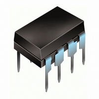
IR2101 International Rectifier, IR2101 Datasheet

IR2101
Specifications of IR2101
Available stocks
Related parts for IR2101
IR2101 Summary of contents
Page 1
... Gate drive supply range from 10 to 20V Undervoltage lockout 3.3V, 5V, and 15V logic input compatible Matched propagation delay for both channels Outputs in phase with inputs (IR2101) or out of phase with inputs (IR2102) Also available LEAD-FREE Description The IR2101(S)/IR2102(S) are high voltage, high speed power MOSFET and IGBT drivers with independent high and low side referenced output channels ...
Page 2
... HO V Low side and logic fixed supply voltage CC V Low side output voltage LO V Logic input voltage (HIN & LIN) (IR2101) & (HIN & LIN) (IR2102 Ambient temperature A Note 1: Logic operational for +600V. Logic state held for V S DT97-3 for more details). ...
Page 3
... COM. The V and I parameters are referenced to COM and are applicable to the respective output leads LO Symbol Definition V Logic “1” input voltage (IR2101) IH Logic “0” input voltage (IR2102) V Logic “0” input voltage (IR2101) IL Logic “1”input voltage (IR2102) V High level output voltage, V ...
Page 4
... S ) IR2101 /IR2102 Functional Block Diagram HIN UV DETECT LIN Vcc HIN UV DETECT Vcc LIN & (PbF) HV LEVEL PULSE SHIFT FILTER PULSE GEN IR2101 HV PULSE LEVEL SHIFT FILTER PULSE GEN IR2102 COM COM www.irf.com ...
Page 5
... Lead Definitions Symbol Description HIN Logic input for high side gate driver output (HO), in phase (IR2101) HIN Logic input for high side gate driver output (HO), out of phase (IR2102) LIN Logic input for low side gate driver output (LO), in phase (IR2101) LIN ...
Page 6
... S ) IR2101 /IR2102 HIN LIN HIN LIN HO LO Figure 1. Input/Output Timing Diagram HIN LIN HIN LIN Figure 3. Delay Matching Waveform Definitions & (PbF) HIN LIN HIN LIN Figure 2. Switching Time Waveform Definitions 50% 50% 50 50% 50% 50% 50 off t f 90% 90% 10% 10% www ...
Page 7
... Input Voltage (V) Figure 6C. Turn-On Time vs Input Voltage 500 400 Max. 300 200 Typ. 100 VBIAS Supply Voltage (V) Figure 7B. Turn-Off Time vs Supply Voltage www.irf.com ( S ) IR2101 500 400 Max. 300 200 Typ. 100 0 75 100 125 10 Figure 6B. Turn-On Time vs Supply Voltage -50 -25 Figure 7A. Turn-Off Time vs Temperature ...
Page 8
... Logic "0" Input Voltage (IR2102) vs Temperature & (PbF Figure 9B. Turn-On Rise Time vs Voltage Figure 10B. Turn-Off Fall Time vs Voltage Figure 12B. Logic "1" Input Voltage (IR2101) Logic "0" Input Voltage (IR2102 VBIAS Supply Voltage ( VBIAS Supply Voltage ( Vcc Supply Voltage (V) vs Voltage www.irf.com 2 0 ...
Page 9
... Temperature (°C) Figure 13A. Logic "0" Input Voltage (IR2101) Logic "1" Input Voltage (IR2102) vs Temperature Temperature (°C) Figure 14A. High Level Output vs Temperature Temperature (°C) Figure 15A. Low Level Output vs Temperature www.irf.com ( S ) IR2101 4 3.2 2 Figure 13B. Logic "0" Input Voltage (IR2101) Logic " ...
Page 10
... S ) IR2101 /IR2102 Temperature (°C) Figure 16A. Offset Supply Current vs Temperature -50 - Temperature (°C) Figure 17A. V Supply Current BS vs Temperature Temperature (°C) Figure 18A. Vcc Supply Current vs Temperature & (PbF) 500 400 300 200 100 Max Figure 16B. Offset Supply Current 150 ...
Page 11
... Max -50 - Temperature (°C) Figure 20A. Logic "0" Input Current vs Temperature 11 M ax. 10 Typ -50 - Temperature (°C) Figure 21A. Vcc Undervoltage Threshold(+) vs Temperature www.irf.com ( S ) IR2101 Figure 19B. Logic"1" Input Current Max 100 125 Figure 20B. Logic "0" Input Current 11 10 Max. 9 Typ. ...
Page 12
... S ) IR2101 /IR2102 500 400 Typ. 300 200 100 Min. 0 -50 - Temperature (°C) Figure 22A. Output Source Current vs Temperature -50 - Temperature (°C) Figure 23A. Output Sink Current vs Temperature & (PbF) 500 400 300 200 Typ. 100 Min 100 125 10 Figure 22B. Output Source Current ...
Page 13
... 0.25 [.010 NOTES: 1. DIMENSIONING & TOLERANCING PER ASME Y14.5M-1994. 2. CONTROLLING DIMENSION: MILLIMETER 3. DIMENSIONS ARE SHOWN IN MILLIMETERS [INCHES]. 4. OUTLINE C ONFORMS TO JEDEC OUTLINE MS-012AA. www.irf.com ( S ) IR2101 8 Lead PDIP FOOTPRINT 8X 0.72 [.028 6.46 [.255] 3X 1.27 [.050] 8X 1.78 [.070 45° 0.10 [.004 DIMENSION DOES NOT INCLUDE MOLD PROTRUSIONS. ...
Page 14
... Assembly site code Per SCOP 200-002 Leadfree Part 8-Lead PDIP IR2101 order IR2101PbF 8-Lead SOIC IR2101S order IR2101SPbF 8-Lead PDIP IR2102 order IR2102PbF 8-Lead SOIC IR2102S order IR2102SPbF This product has been qualified per industrial level Data and specifications subject to change without notice. ...


