IR2104 International Rectifier, IR2104 Datasheet
IR2104
Specifications of IR2104
Available stocks


Related parts for IR2104

IR2104 Summary of contents
Page 1
... Shut down input turns off both channels Matched propagation delay for both channels Also available LEAD-FREE Description The IR2104(S) are high voltage, high speed power MOSFET and IGBT drivers with dependent high and low side referenced output channels. Proprietary HVIC and latch immune CMOS technologies enable ruggedized monolithic construction ...
Page 2
... S ) & (PbF) IR2104 Absolute Maximum Ratings Absolute maximum ratings indicate sustained limits beyond which damage to the device may occur. All voltage parameters are absolute voltages referenced to COM. The thermal resistance and power dissipation ratings are measured under board mounted and still air conditions. ...
Page 3
... BIAS O — — O — — — 30 — 150 — — — 8 8.9 7.4 8.2 130 210 270 360 ( S ) & (PbF) IR2104 820 220 V = 600V S 220 170 ns 90 650 60 and I parameters are referenced to IN — 10V to 20V CC 0 10V to 20V ...
Page 4
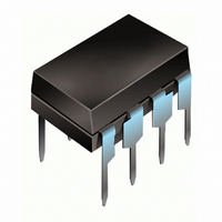
... High side floating supply return S V Low side and logic fixed supply CC LO Low side gate drive output COM Low side return Lead Assignments COM 8 Lead PDIP IR2104 4 HV LEVEL SHIFT PULSE FILTER PULSE GEN UV DETECT VCC LO COM COM 8 Lead SOIC IR2104S www.irf.com ...
Page 5
... Figure 1. Input/Output Timing Diagram SD 50 90% LO Figure 3. Shutdown Waveform Definitions IN (LO) 50% 50% IN (HO 10% MT 90% Figure 5. Delay Matching Waveform Definitions www.irf.com IN (LO) IN (HO Figure 2. Switching Time Waveform Definitions Figure 4. Deadtime Waveform Definitions & (PbF) IR2104 50% 50% t off 90% 90% 10% 10% 50% 50% 90% 10 90% 10% 5 ...
Page 6
... S ) & (PbF) IR2104 -50 - Temperature (°C) Figure 6A. Turn-On Time vs Temperature 1000 Max. 800 600 . Typ 400 200 Input Voltage (V) Figure 6C. Turn-On Time vs Input Voltage 500 400 Max. 300 200 Typ. 100 VBIAS Supply Voltage (V) Figure 7B. Turn-Off Time vs Supply Voltage 6 1400 1200 Max ...
Page 7
... Figure 10A. Turn-Off Fall Time vs Temperature www.irf.com 500 400 Max. 300 200 Typ. 100 Figure 8B. Shutdown Time vs Voltage Figure 9B. Turn-On Rise Time vs Voltage Figure 10B. Turn-Off Fall Time vs Voltage ( S ) & (PbF) IR2104 VBIAS Supply Voltage ( VBIAS Supply Voltage ( VBIAS Supply Voltage ( ...
Page 8
... S ) & (PbF) IR2104 Temperature (°C) Figure 11A. Deadtime vs Temperature -50 - Temperature (°C) Figure 12A. Logic "1" (HO) & Logic “0” (LO) & Inactive SD Input Voltage vs Temperature 4 3.2 2.4 1.6 Max. 0.8 0 -50 - Temperature (°C) Figure 13A. Logic "0" (HO) & Logic “1” (LO) & ...
Page 9
... Figure 14B. High Level Output vs Voltage Figure 15B. Low level Output vs Voltage 500 400 300 200 100 Max Figure 16B. Offset Supply Current ( S ) & (PbF) IR2104 Vcc Supply Voltage ( Vcc Supply Voltage (V) 100 200 300 400 500 VB Boost Voltage (V) vs Voltage 600 9 ...
Page 10
... S ) & (PbF) IR2104 -50 - Temperature (°C) Figure 17A. V Supply Current BS vs Temperature Temperature (°C) Figure 18A. Vcc Supply Current vs Temperature Temperature (°C) Figure 19A. Logic"1" Input Current vs Temperature 10 150 120 90 60 Max . Figure 17B Figure 18B. Vcc Supply Current vs Voltage Figure 19B. Logic"1" Input Current ...
Page 11
... Figure 20B. Logic "0" Input Current 11 10 Max. 9 Typ Min. 6 -50 -25 75 100 125 Figure 21B. Vcc Undervoltage Threshold(-) 100 125 1 0 Figure 22B. Output Source Current ( S ) & (PbF) IR2104 VCC Supply Voltage (V) vs Voltage 100 125 Temperature (°C) vs Temperature VBIAS Supply Voltage (V) vs Voltage 11 ...
Page 12
... S ) & (PbF) IR2104 -50 - Temperature (°C) Figure 23A. Output Sink Current vs Temperature Case Outlines Figure 23B. Output Sink Current vs Voltage 8 Lead PDIP VBIAS Supply Voltage (V) 01-6014 01-3003 01 (MS-001AB) www.irf.com ...
Page 13
... DIMENSION DOES NOT INCLUDE MOLD PROTRUSIONS. MOLD PROTRUSIONS NOT TO EXCEED 0.15 [.006]. 6 DIMENSION DOES NOT INCLUDE MOLD PROTRUSIONS. MOLD PROTRUSIONS NOT TO EXCEED 0.25 [.010]. 7 DIMENSION IS THE LENGTH OF LEAD FOR SOLDERING TO A SUBSTRATE. 8 Lead SOIC ( S ) & (PbF) IR2104 INCHES MILLIMETERS DIM MIN MAX MIN MAX A ...
Page 14
... SPN code) Assembly site code Per SCOP 200-002 ORDER INFORMATION Leadfree Part 8-Lead PDIP IR2104 order IR2104PbF 8-Lead SOIC IR2104S order IR2104SPbF This product has been qualified per industrial level Data and specifications subject to change without notice. IR logo Lot Code 4/2/2004 ...