IR21531D International Rectifier, IR21531D Datasheet
IR21531D
Specifications of IR21531D
Available stocks


Related parts for IR21531D


IR21531D Summary of contents
Page 1
... Lower power level-shifting circuit Constant LO, HO pulse widths at startup Lower di/dt gate driver for better noise immunity Low side output in phase with R Internal 50nsec (typ.) bootstrap diode (IR21531D) Excellent latch immunity on all inputs and outputs ESD protection on all leads Also available LEAD-FREE ...
Page 2
IR21531(D)(S) & (PbF) Absolute Maximum Ratings Absolute maximum ratings indicate sustained limits beyond which damage to the device may occur. All voltage param- eters are absolute voltages referenced to COM, all currents are defined positive into any lead. The thermal ...
Page 3
Recommended Component Values Symbol Component R Timing resistor value pin capacitor value T T 1000000 100000 330pf 10000 470pF 1nF 1000 2.2nF 4.7nF 10nF 100 10 10 100 www.irf.com IR21531(D)(S) & (PbF) IR21531 RT vs Frequency IR2153 ...
Page 4
... QBSUV BS I Quiescent VBS supply current QBS V Minimum required V voltage for proper BSMIN BS functionality from Offset supply leakage current LK V Bootstrap diode forward voltage (IR21531D) F Oscillator I/O Characteristics Symbol Definition f osc Oscillator frequency d R pin duty cycle pin current UV-mode C pin pulldown current ...
Page 5
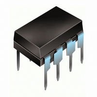
... Low side gate driver output V High voltage floating supply return S HO High side gate driver output V High side gate driver floating supply B Lead Assignments 8 Lead DIP IR21531(D) NOTE: The IR21531D is offered in 8 lead DIP only. www.irf.com IR21531(D)(S) & (PbF) Min. Typ. -V — 0 BIAS O — 0 — ...
Page 6
... IR21531(D)(S) & (PbF) Functional Block Diagram for IR21531( R R/2 LOGIC UV DETECT Functional Block Diagram for IR21531D R R/2 LOGIC UV DETECT NOTE: The separate die LEVEL PULSE SHIFT FILTER DEAD PULSE TIME GEN DELAY DEAD TIME HV LEVEL PULSE SHIFT FILTER DEAD PULSE TIME ...
Page 7
IR21531(D)(S) & (PbF) 8 Lead PDIP 8 Lead SOIC 01-3003 01 01-0021 08 7 ...
Page 8
IR21531(D)(S) & (PbF) Vccuv+ Vcc 2 1 Figure 1. Input/Output Timing Diagram (HO) (LO) Figure 2. Switching Time Waveform Definitions 8 V CLAMP 50% 50% 90% ...
Page 9
... Per SCOP 200-002 ORDER INFORMATION Leadfree Part 8-Lead PDIP IR21531 order IR21531PbF 8-Lead SOIC IR21531S order IR21531SPbF 8-Lead PDIP IR21531D order IR21531DPbF This product has been qualified per industrial level Data and specifications subject to change without notice. IR logo Lot Code 9/20/2005 ...