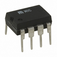
MIC4452BN Micrel Inc, MIC4452BN Datasheet - Page 3

MIC4452BN
Manufacturer Part Number
MIC4452BN
Description
IC DRIVER MOSF 12A LO SIDE 8DIP
Manufacturer
Micrel Inc
Datasheet
1.MIC4452YM_TR.pdf
(14 pages)
Specifications of MIC4452BN
Configuration
Low-Side
Input Type
Non-Inverting
Delay Time
15ns
Current - Peak
12A
Number Of Configurations
1
Number Of Outputs
1
Voltage - Supply
4.5 V ~ 18 V
Operating Temperature
-40°C ~ 85°C
Mounting Type
Through Hole
Package / Case
8-DIP (0.300", 7.62mm)
Device Type
MOSFET
Driver Case Style
DIP
No. Of Pins
8
Operating Temperature Range
-40°C To +85°C
Power Dissipation Pd
960mW
Termination Type
Through Hole
Rise Time
20ns
Peak Output High Current, Ioh
12A
Lead Free Status / RoHS Status
Contains lead / RoHS non-compliant
High Side Voltage - Max (bootstrap)
-
Lead Free Status / RoHS Status
Contains lead / RoHS non-compliant, Contains lead / RoHS non-compliant
Absolute Maximum Ratings
Supply Voltage ..............................................................20V
Input Voltage .................................... V
Input Current (V
Power Dissipation, T
Power Dissipation, T
Derating Factors (to Ambient)
Storage Temperature ................................−65°C to +150°C
Lead Temperature(10 sec) ........................................ 300°C
Electrical Characteristics
(T
Micrel Inc.
Symbol
Input
V
V
V
I
Output
V
V
R
R
I
I
I
Switching Time
t
t
t
t
Power Supply
I
V
January 2011
IN
PK
DC
R
R
F
D1
D2
S
A
IH
IL
IN
OH
OL
S
O
O
=25
PDIP ..................................................................960mW
SOIC ................................................................1040mW
5-Pin TO-220 ............................................................2W
5-Pin TO-220 .......................................................12.5W
PDIP ..............................................................7.7mW/°C
SOIC ..............................................................8.3mW/°C
5-Pin TO-220 ..................................................17mW/°C
o
C, with 4.5V ≤ V
Parameter
Logic 1 Input Voltage
Logic 0 Input Voltage
Input Voltage Range
Input Current
High Output Voltage
Low Output Voltage
Output Resistance,
Output High
Output Resistance, Output Low
Peak Output Current
Continuous Output Current
Latch-up Protection
Withstand Reverse Current
Rise Time
Fall Time
Delay Time
Delay Time
Power Supply Current
Operating Input Voltage
IN
(3)
> V
AMBIENT
CASE
S
S
) .................................................5mA
≤ 18V unless otherwise specified.)
≤ 25°C
≤ 25°C
(4)
S
(1,2, 3)
+ 0.3V to GND −5V
Condition
0 ≤ V
See Figure 1
See Figure 1
I
I
V
Duty Cycle ≤ 2%
t ≤ 300μs
Test Figure 1, C
Test Figure 1, C
Test Figure 1
Test Figure 1
V
V
OUT
OUT
S
IN
IN
= 18V (See Figure 6)
= 3V
= 0V
= 10mA, V
= 10mA, V
IN
≤ V
S
S
S
L
L
= 18V
= 18V
= 15,000pF
= 15,000pF
3
Operating Ratings
Operating Temperature (Chip) .................................. 150°C
Operating Temperature (Ambient)
Thermal Impedances (To Case)
Z Version .................................................. 0°C to +70°C
Y Version ............................................. −40°C to + 85°C
5-Pin TO-220(θJC) ........................................... 10°C/W
V
>1500
S
Min.
−10
2.4
−.025
4.5
−5
2
Typ.
1.3
1.1
0.6
0.8
0.4
12
20
24
25
40
80
V
MIC4451/4452
Max.
.025
S
150
0.8
1.5
1.5
1.5
M9999-011811
10
40
50
50
60
+ .3
Units
mA
mA
μA
μA
ns
ns
ns
ns
Ω
Ω
V
V
V
V
V
A
A
V


