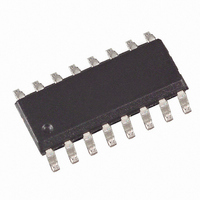
T6819-TBQ Atmel, T6819-TBQ Datasheet - Page 9

T6819-TBQ
Manufacturer Part Number
T6819-TBQ
Description
IC DRIVER DUAL TRPL DMOS 16-SOIC
Manufacturer
Atmel
Type
High Side/Low Side Driverr
Datasheet
1.T6819-TBQ.pdf
(16 pages)
Specifications of T6819-TBQ
Input Type
Serial
Number Of Outputs
6
On-state Resistance
500 mOhm
Current - Output / Channel
1.5A
Current - Peak Output
2A
Voltage - Supply
7 V ~ 40 V
Operating Temperature
-40°C ~ 150°C
Mounting Type
Surface Mount
Package / Case
16-SOIC (3.9mm Width)
For Use With
ATAB6819 - BOARD EVAL FOR T6819/ATA6829
Lead Free Status / RoHS Status
Contains lead / RoHS non-compliant
Other names
T6819-TBQTR
Electrical Characteristics (Continued)
7.5 V < V
4531D–BCD–07/04
*) Type means: A =100% tested, B = 100% correlation tested, C = Characterized on samples, D = Design parameter
Note:
4.10
4.11
4.12
4.13
4.14
No.
3.5
3.6
3.7
3.8
4.1
4.2
4.3
4.4
4.5
4.6
4.7
4.8
4.9
4
S
1. Delay time between rising edge of input signal at pin CS after data transmission and switch on/off output stages to 90% of
2. Delay time between rising/falling edge of input signal at pin PWM and switch on/off output stages to 90% of final level.
3. Difference between switch-on and switch-off delay time of input signal at pin PWM to output stages in PWM mode.
Parameters
Thermal shutdown on
Thermal shutdown
hysteresis
Ratio thermal shutdown
off/thermal prewarning
set
Ratio thermal shutdown
on/thermal prewarning
reset
Output Specification (OUT1-OUT3)
On resistance
High-side output
leakage current
Low-side output
leakage current
High-side switch
reverse diode forward
voltage
Low-side switch
reverse diode forward
voltage
High-side overcurrent
limitation and shutdown
threshold
Low-side overcurrent
limitation and shutdown
threshold
Overcurrent shutdown
delay time
High-side open load
detection current
Low-side open load
detection current
High-side output switch
on delay
Low-side output switch
on delay
High-side output switch
off delay
< 40 V; 4.75 V < V
final level. Device not in standby for t > 1 ms.
(1),(2)
(1),(2)
(1),(2)
CC
< 5.25 V; INH = High; -40° C < T
Test Conditions
I
I
V
output stages off
V
output stages off
I
I
Input register bit 13
(OLD) = low, output off
Input register bit 13
(OLD) = low, output off
R
R
V
R
Out 1-3 H
Out 1-3 L
Out
Out 1-3 L
V
V
Out 1-3 H
Out 1-3 L
VS
Load
Load
Load
VS
VS
= 1.5 A
=13 V
= 13 V
= 13 V
= 30 Ω
= 30 Ω
= 30 Ω
= 1.3 A
= -1.5 A
= -1.3 A
= V
= 0 V
VS,
,
2, 3, 15
2, 3, 15
2, 3, 15
2, 3, 15
2, 3, 15
4, 13,
4, 13,
4, 13,
4, 13,
4, 13,
Pin
14
14
14
14
14
j
< 150° C; unless otherwise specified, all values refer to GND pins.
V
∆T
R
T
T
R
Out1-3
T
T
Symbol
V
T
I
I
I
j switch off/
j switch on/
I
I
I
j switch on
DSOn1-3H
DSOn1-3L
jPW reset
Out1-3H
Out1-3H
Out1-3H
Out1-3L
Out1-3L
Out1-3L
j switch off
Out1-3L
jPW set
t
t
t
t
dSd
don
don
doff
- V
VS
T6819/T6829 [Preliminary]
Min.
1.05
1.05
-1.5
-2.5
-2.5
135
1.5
0.2
10
-5
Typ.
160
1.2
1.2
15
-2
2
Max.
185
-1.5
-0.2
1.1
1.1
1.5
2.5
2.5
40
20
20
20
5
Unit
mA
mA
° C
µA
µA
µs
µs
µs
µs
K
Ω
Ω
V
V
A
A
Type*
B
B
B
B
A
A
A
A
A
A
A
A
A
A
A
A
A
A
9


