ATA6829-T3QY 71 Atmel, ATA6829-T3QY 71 Datasheet - Page 3
ATA6829-T3QY 71
Manufacturer Part Number
ATA6829-T3QY 71
Description
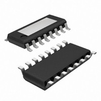
IC DRIVER TRPL HALFBRIDGE 16PSOP
Manufacturer
Atmel
Type
High Side/Low Side Driverr
Datasheet
1.ATA6829-T3QY_71.pdf
(16 pages)
Specifications of ATA6829-T3QY 71
Input Type
Serial
Number Of Outputs
6
On-state Resistance
1.1 Ohm
Current - Peak Output
2A
Voltage - Supply
5.6 V ~ 40 V
Operating Temperature
-40°C ~ 150°C
Mounting Type
Surface Mount
Package / Case
16-PSOP
Product
Half-Bridge Drivers
Rise Time
100 ns
Fall Time
100 ns
Supply Voltage (max)
40 V
Supply Current
350 uA
Maximum Operating Temperature
+ 150 C
Mounting Style
SMD/SMT
Minimum Operating Temperature
- 55 C
Number Of Drivers
3
Output Current
- 10 A to + 10 A
Output Voltage
40 V
Lead Free Status / RoHS Status
Lead free / RoHS Compliant
Current - Output / Channel
-
Lead Free Status / Rohs Status
Lead free / RoHS Compliant


2. Pin Configuration
Figure 2-1.
Table 2-1.
4531G–BCD–07/09
Pin
10
11
12
13
14
15
16
1
2
3
4
5
6
7
8
9
Pinning PSO16
Pin Description
Symbol
OUT3H
OUT1H
OUT2H
OUT1L
OUT3L
OUT2L
PWM
GND
GND
GND
VCC
CLK
CS
DO
VS
DI
Function
Ground; reference potential; internal connection to pin 9 and pin 16; connection to heat slug
Low-side driver output 1; power MOS open drain with internal reverse diode; short-circuit protection;
overtemperature protection; diagnosis for short and open load; PWM ability
Low-side driver output 3; see pin 2
High-side driver output 3; power MOS open source with internal reverse diode; short-circuit protection;
overtemperature protection; diagnosis for short and open load; PWM ability
Chip select input; 5-V CMOS logic level input with internal pull up;
low = serial communication is enabled, high = disabled
Serial data input; 5-V CMOS logic level input with internal pull down; receives serial data from the control
device; DI expects a 16-bit control word with LSB being transferred first
Serial clock input; 5-V CMOS logic level input with internal pull down; controls serial data input interface
and internal shift register (f
PWM input; 5-V CMOS logic level input with internal pull down; receives PWM signal to control outputs
which are selected for PWM mode by the serial data interface, high = outputs on, low = outputs off
Ground; see pin 1
Serial data output; 5-V CMOS logic-level tri-state output for output (status) register data; sends 16-bit
status information to the microcontroller (LSB is transferred first); output will remain tri-stated unless
device is selected by CS = low, therefore, several ICs can operate on one data-output line only.
Logic supply voltage (5V)
Power supply for high-side output stages OUT1H, OUT2H, OUT3H, internal supply
High-side driver output 1; see pin 4
High-side driver output 2; see pin 4
Low-side driver output 2; see pin 2
Ground; see pin 1
OUT3H
OUT1L
OUT3L
PWM
GND
CLK
max
CS
DI
= 2 MHz)
1
2
3
4
5
6
7
8
16
15
14
13
12
11
10
9
GND
OUT2L
OUT2H
OUT1H
VS
VCC
DO
GND
ATA6829
3
Related parts for ATA6829-T3QY 71
Image
Part Number
Description
Manufacturer
Datasheet
Request
R

Part Number:
Description:
IC DRIVER TRPL HALFBRIDGE 16PSOP
Manufacturer:
Atmel
Datasheet:

Part Number:
Description:
Dual Triple DMOS Output Driver with Serial Input Control
Manufacturer:
ATMEL Corporation
Datasheet:
Part Number:
Description:
MOSFET & Power Driver ICs Triple Half-Bridge Driver
Manufacturer:
Atmel
Datasheet:

Part Number:
Description:
DEV KIT FOR AVR/AVR32
Manufacturer:
Atmel
Datasheet:
Part Number:
Description:
INTERVAL AND WIPE/WASH WIPER CONTROL IC WITH DELAY
Manufacturer:
ATMEL Corporation
Datasheet:
Part Number:
Description:
Low-Voltage Voice-Switched IC for Hands-Free Operation
Manufacturer:
ATMEL Corporation
Datasheet:
Part Number:
Description:
MONOLITHIC INTEGRATED FEATUREPHONE CIRCUIT
Manufacturer:
ATMEL Corporation
Datasheet:
Part Number:
Description:
AM-FM Receiver IC U4255BM-M
Manufacturer:
ATMEL Corporation
Datasheet:
Part Number:
Description:
Monolithic Integrated Feature Phone Circuit
Manufacturer:
ATMEL Corporation
Datasheet:
Part Number:
Description:
Multistandard Video-IF and Quasi Parallel Sound Processing
Manufacturer:
ATMEL Corporation
Datasheet:
Part Number:
Description:
High-performance EE PLD
Manufacturer:
ATMEL Corporation
Datasheet:
Part Number:
Description:
8-bit Flash Microcontroller
Manufacturer:
ATMEL Corporation
Datasheet: