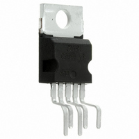
VN920-E STMicroelectronics, VN920-E Datasheet - Page 8

VN920-E
Manufacturer Part Number
VN920-E
Description
IC DRIVER HIGH SIDE PENTAWATT-5
Manufacturer
STMicroelectronics
Type
High Sider
Datasheet
1.VN920B5TR-E.pdf
(23 pages)
Specifications of VN920-E
Input Type
Non-Inverting
Number Of Outputs
1
On-state Resistance
16 mOhm
Current - Output / Channel
45A
Voltage - Supply
5.5 V ~ 36 V
Operating Temperature
-40°C ~ 150°C
Mounting Type
Through Hole
Package / Case
Pentawatt-5 (Vertical, Bent and Staggered Leads)
Switch Type
High Side
Power Switch Family
VN920
Power Switch On Resistance
16mOhm
Output Current
30A
Mounting
Through Hole
Supply Current
5mA
Package Type
Pentawatt
Operating Temperature (min)
-40C
Operating Temperature (max)
150C
Operating Temperature Classification
Automotive
Pin Count
5 +Tab
Power Dissipation
96.1W
Supply Voltage (min)
5.5 V
Maximum Power Dissipation
96100 mW
Maximum Operating Temperature
+ 150 C
Mounting Style
Through Hole
Minimum Operating Temperature
- 40 C
Device Type
High Side
Module Configuration
High Side
Peak Output Current
45A
Output Resistance
0.016ohm
Input Delay
50µs
Output Delay
50µs
Supply Voltage Range
5.5V To 36V
Rohs Compliant
Yes
Lead Free Status / RoHS Status
Lead free / RoHS Compliant
Current - Peak Output
-
Lead Free Status / Rohs Status
Compliant
Electrical specifications
8/23
Table 5.
1. V
Table 6.
Table 7.
Table 8.
Table 9.
dV
dV
Symbol
Symbol
Symbol
V
Symbol
I
I
I
Symbol
L(off2)
L(off3)
L(off4)
V
T
OUT
OUT
I(hyst)
T
V
V
I
I
I
t
t
T
IH
ICL
TSD
clamp
IL
V
hyst
IH
lim
d(on)
d(off)
IL
R
F
/dt
/dt
and V
(on)
(off)
Off-state output current
Off-state output current
Off-state output current
Input low level voltage
Low level input current
Input high-level voltage
High-level input current
Input hysteresis voltage
Input clamp voltage
Shutdown temperature
Reset temperature
Thermal hysteresis
DC short circuit current
Power (continued)
Switching (V
Logic inputs
V
Protections
Forward on voltage
Turn-on delay time
Turn-off delay time
Turn-on voltage slope R
Turn-off voltage slope R
OV
CC
are correlated. Typical difference is 5V.
Parameter
Parameter
Parameter
output diode
Parameter
Parameter
(1)
CC
=13V)
Doc ID 10894 Rev 3
- I
V
5V < V
V
V
V
V
V
R
R
CC
OUT
IN
IN
CC
IN
CC
L
L
L
L
= 1.3Ω (see
= 1.3Ω (see
= 1.3Ω (see
= 1.3Ω (see
V
V
I
I
= V
= V
= V
= 13V
Test conditions
IN
IN
= 13V; T
= 13V; T
Test conditions
IN
IN
= 2A; T
CC
= 1mA
= - 1mA
OUT
OUT
OUT
= 1.25V
= 3.25V
Test conditions
< 36V
Test conditions
Test conditions
= V
= V
= V
j
j
j
= 150°C
= 125°C
= 25°C
SENSE
SENSE
SENSE
Figure
Figure
Figure
Figure
= 3.5V
= 0V;
= 0V;
5)
5)
5)
5)
Min.
-
-
-
-
Min.
150
135
30
7
Min.
3.25
See
See
0.5
1
6
Min.
Min.
-75
-
Figure 15
Figure 16
Typ.
Typ.
175
50
50
15
45
Typ.
- 0.7
6.8
Typ.
Typ.
-
Max.
Max.
1.25
Max.
200
10
75
75
Max. Unit
Max. Unit
0.6
8
-
-
-
-
5
3
VN920-E
Unit
Unit
V/µs
V/µs
Unit
µA
µA
µA
µA
µA
°C
µs
µs
V
V
V
V
V
°C
°C
V
A
A


